










PCB Knowledge
Printed circuit boards (PCBs) form the backbone of modern electronics, enabling everything from smartphones to industrial machinery. In our PCB Knowledge category, we delve into the essential principles, techniques, and innovations that drive this field forward. Whether you are an engineer refining your designs or a hobbyist embarking on your first project, this collection offers valuable resources to enhance your understanding and skills. The scope of PCB Knowledge spans foundational concepts such as circuit layout and component selection, extending to advanced topics like high-speed signal integrity and thermal management. We provide detailed guides that walk through design software usage, manufacturing processes, and quality assurance methods. Tutorials offer hands-on instructions for prototyping and assembly, while insights from industry experts share real-world case studies and emerging trends. Best practices emphasize reliability, cost efficiency, and compliance with standards like IPC, ensuring your projects meet professional benchmarks. The practical value lies in its direct applicability to everyday challenges. For instance, articles on troubleshooting common PCB failures can save time and resources in product development cycles. Discussions on materials science reveal how choices in substrates and coatings impact performance in harsh environments, such as automotive or aerospace applications. By addressing these elements, PCB Knowledge equips you with tools to innovate and optimize electronic systems that power renewable energy solutions, medical devices, and consumer gadgets. As you read through the articles here, you will gain a comprehensive perspective that connects theoretical knowledge with tangible outcomes. This category serves as a hub for ongoing learning, where each piece builds on the others to foster expertise in PCB technology. Stay informed on the latest advancements, from flexible PCBs to sustainable manufacturing, and apply these insights to your work for superior results.
Latest Blogs
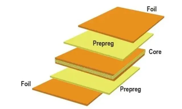
What Do 7628, 1080, and 2116 Mean in a PCB? Understanding These Numbers Means Understanding the Stack-Up
Understand PCB glass-fabric codes 7628, 1080, 2116, 3313, 1078, and 1506, plus how prepreg, resin content, lamination, and fiber weave affect stack-up design.
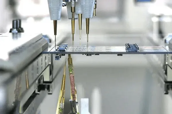
PCB Power Stability Testing
Power-output testing covers overshoot, undershoot, glitches, dips, sags, and surges, with procedures for evaluating transients and selecting inductors and capacitors.
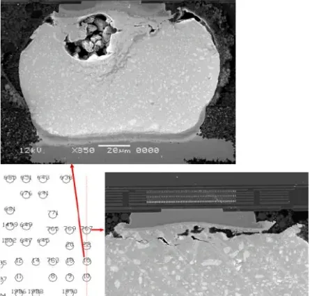
Temperature Is a Major Threat to Reliability
Learn how temperature affects component failure rates, derating, temperature cycling, parameter drift, BGA solder reliability, and thermal monitoring and protection.

Four-Corner Testing: A Rigorous Method for Hardware Reliability Verification
Explore four-corner testing for PCB and DDR3 reliability, covering temperature, supply-voltage extremes, stress workloads, ECC monitoring, and operating-margin analysis.

Why Are Conductive Polymer Capacitors Being Used More Frequently?
Compare conductive polymer capacitors with MLCCs, aluminum electrolytic, and tantalum capacitors for stable capacitance, lower component count, and reduced acoustic noise.

Complete Guide to Power-Rail Ripple and Noise Testing: From Principles to Practice
Compare six power-rail ripple and noise measurement methods, identify oscilloscope setup errors, and apply a repeatable procedure for accurate, consistent results.

IPC-1601A: Guide for Handling, Packaging, Storage, and Transportation of Printed Circuit Boards
IPC-1601A provides guidelines for PCB handling, ESD protection, packaging, storage, transportation, and inspection to preserve board quality and reliability.

MOSFET: The Electronic Water Gate Hidden Inside Every Chip
Explore how MOSFETs control current, build logic gates, store data, route signals, manage power, and amplify analog signals in modern electronics.

What Is the Engineering Basis of the 3W Rule?
Explore the PCB 3W rule, its role in reducing crosstalk, and practical methods such as grounding, stackup design, termination, and SI simulation when spacing is limited.

Encapsulant (Encap) Process Requirements and Operating Guidelines
Learn PCB encapsulant process requirements, including cold storage, temperature recovery, dispensing, curing, quality inspection, and component rework.

IPC-1602 Standard for the Handling and Storage of Printed Boards
IPC-1602 defines PCB handling, moisture control, bake-out, packaging, storage, transportation, ESD protection, and solderability requirements.

Why Do Eye Diagrams Collapse Even When High-Speed Interface Traces Are Length-Matched?
Length-matched high-speed traces can still fail if the return path is discontinuous; analyze reference plane continuity to reduce reflections and jitter.


