 00:50
00:50
Component Placement
Component placement is a critical aspect of printed circuit board (PCB) design that directly influences the functionality, reliability, and manufacturability of electronic assemblies. When engineers and designers search for guidance on component placement, they often seek strategies to optimize board layout for better signal integrity, thermal management, and ease of assembly. This tag encompasses a range of topics, from fundamental principles to advanced techniques, helping users address common challenges such as minimizing electromagnetic interference, reducing trace lengths for high-speed signals, and ensuring adequate spacing for heat dissipation. In practice, effective component placement begins with understanding the schematic and prioritizing components based on their roles. For instance, placing sensitive analog components away from noisy digital sections can prevent crosstalk, while grouping power regulators near high-current loads improves efficiency and reduces voltage drops. Best practices also include considering mechanical constraints, such as connector positions for user interfaces or mounting holes for enclosures, to streamline the transition from design to production. By adhering to these guidelines, designers can avoid costly revisions and enhance overall board performance, whether working on consumer electronics, automotive systems, or industrial controls. For those delving deeper into specific scenarios, articles under this tag offer detailed case studies and step-by-step tutorials. You might find insights on automating placement with CAD software or troubleshooting issues in multilayer boards, providing the tools needed to refine your designs. As PCB complexity grows with emerging technologies like IoT and 5G, mastering component placement remains essential for achieving robust, high-performing circuits.
Video Guide

Technical Articles
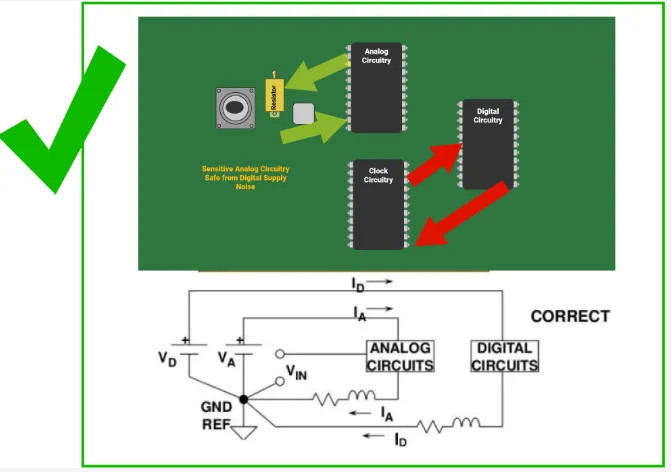
The Impact of Component Orientation on PCB Signal Integrity and Performance
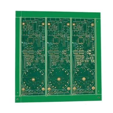
Optimizing PCB Design: V-Scoring, Component Placement, and Reliability
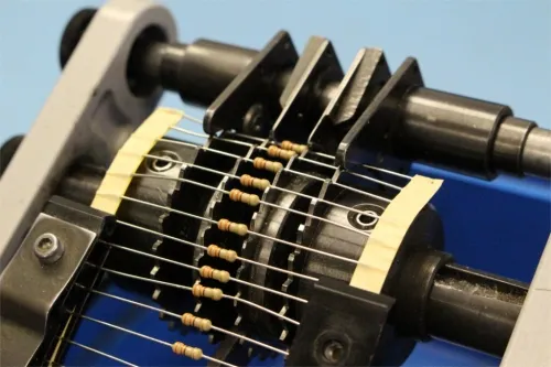
Essential Guide to Component Lead Forming for Robust PCB Assembly
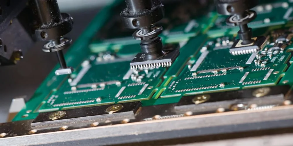
Component Placement Strategies for High Volume Assembly
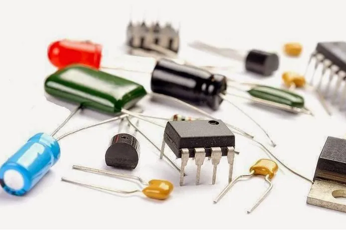
Basic Electronic Components Guide: Identifying Common PCB Parts for Beginners
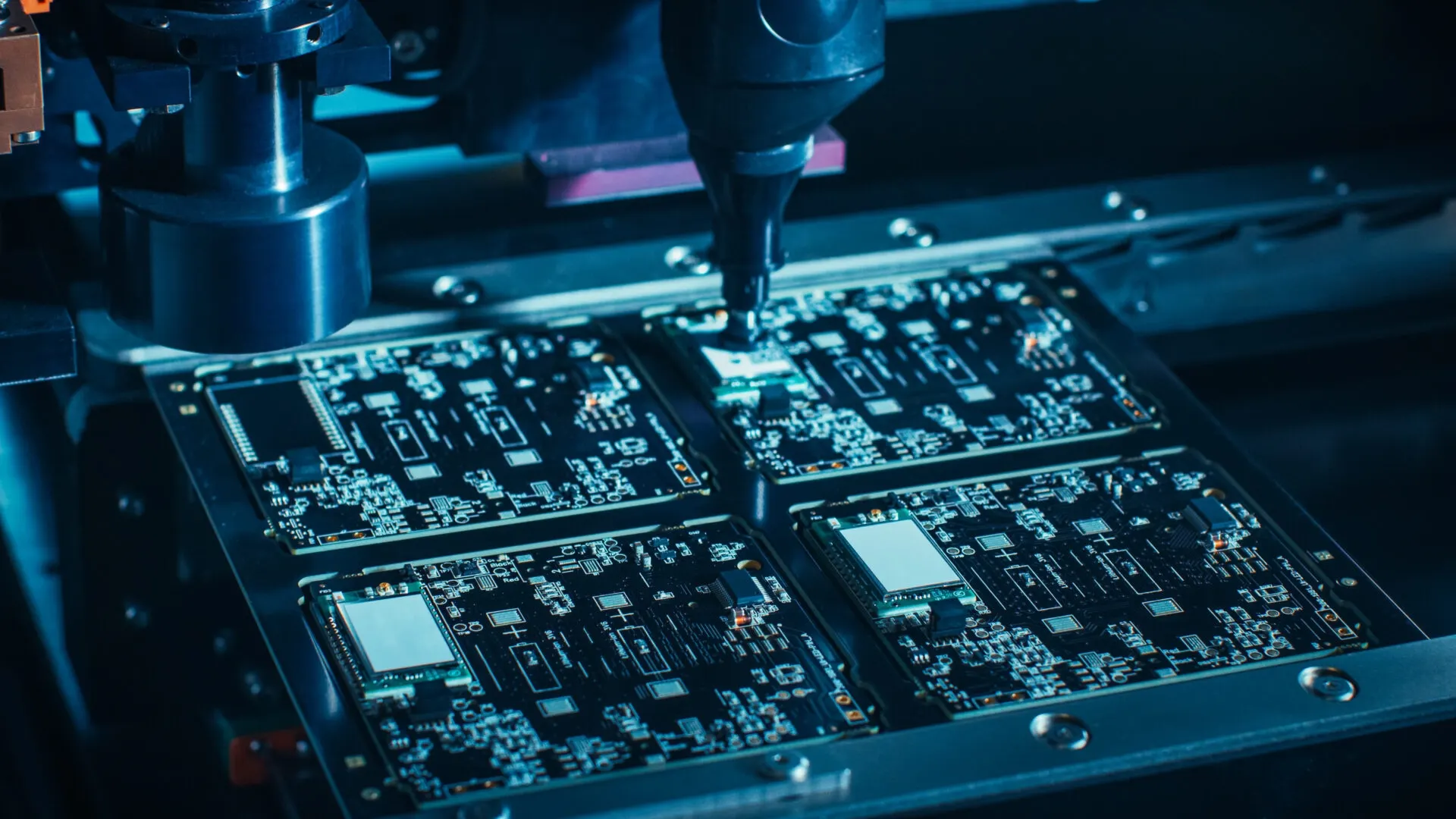
PCB Prototype Design for Manufacturability (DFM): Avoiding Costly Errors

Custom PCB Design for Agriculture: A Guide to Automated Irrigation Systems
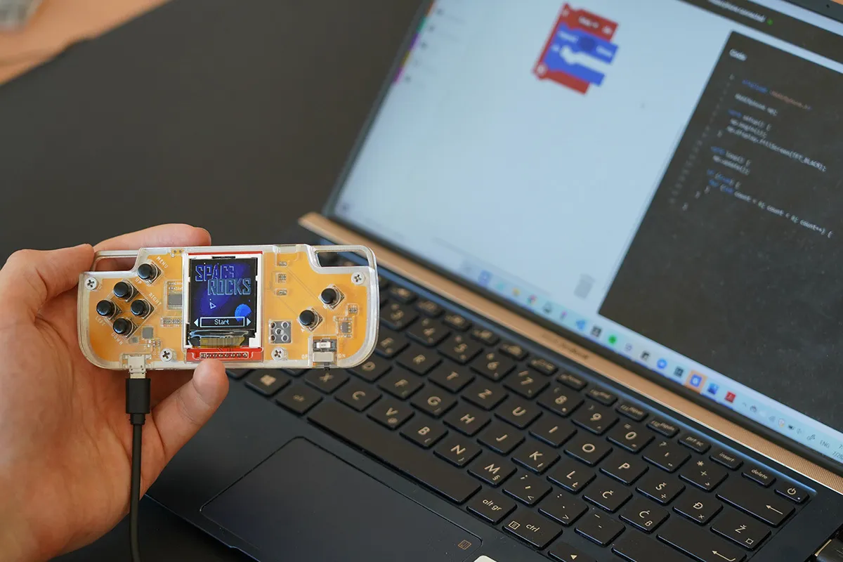
Building a Portable Game Console: A DIY PCB Project Guide
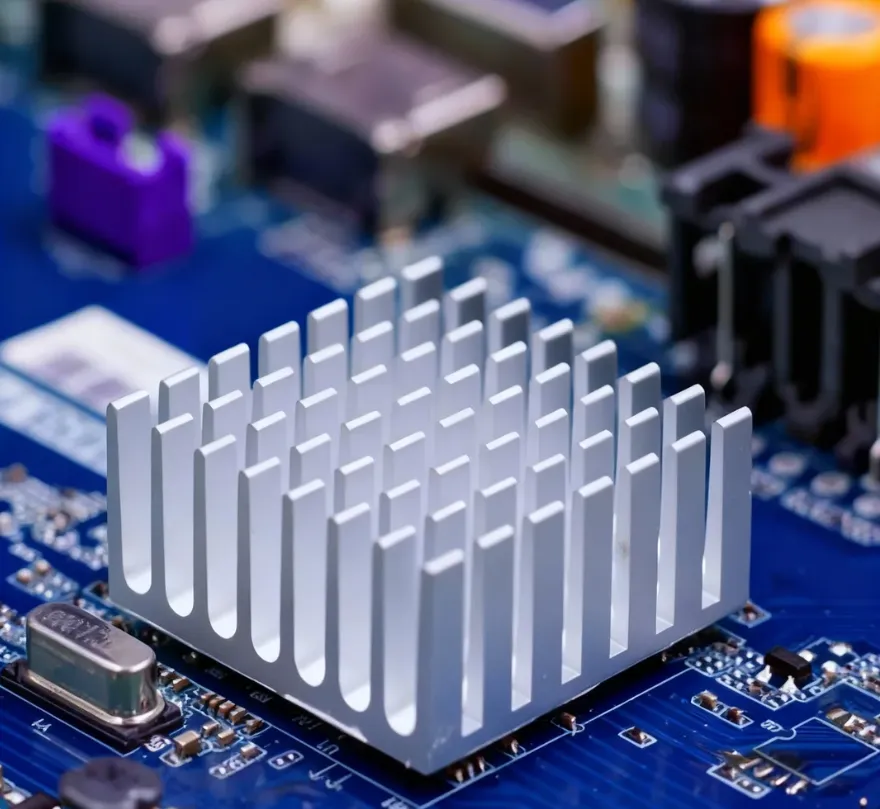
Mastering SMT Component Placement for Optimal PCB Design
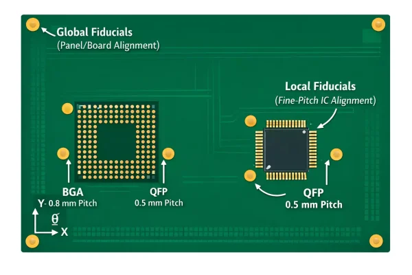
FR4 PCB Fiducial Design: Placement Rules for Reliable Assembly
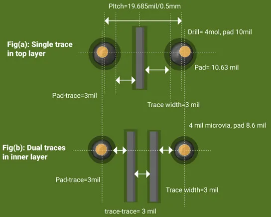
Component Placement Mistakes That Make HDI PCB Routing Harder
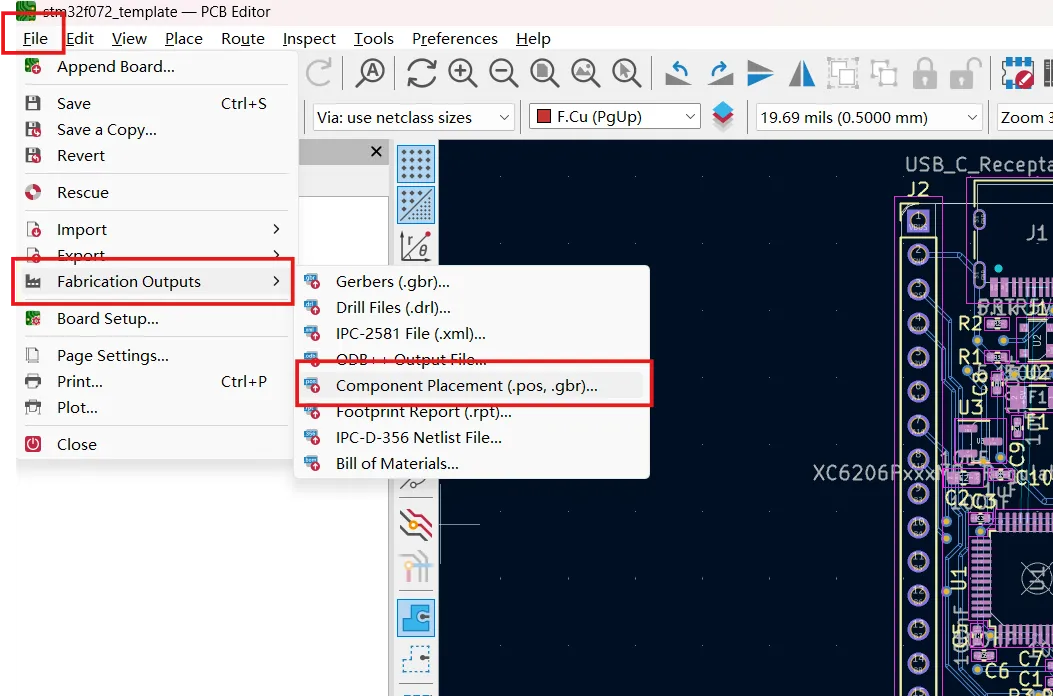
Generating Pick-and-Place Files in KiCad: Complete SMT Assembly Guide
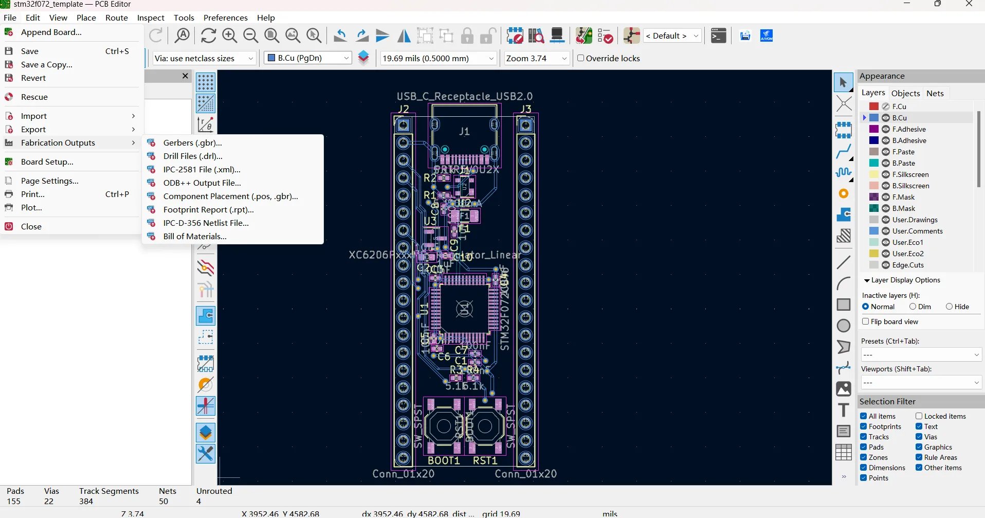
How to Prepare KiCad Files for PCB Assembly: Gerber, BOM and Pick-and-Place Guide
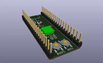
PCB Component Placement Best Practices in KiCad
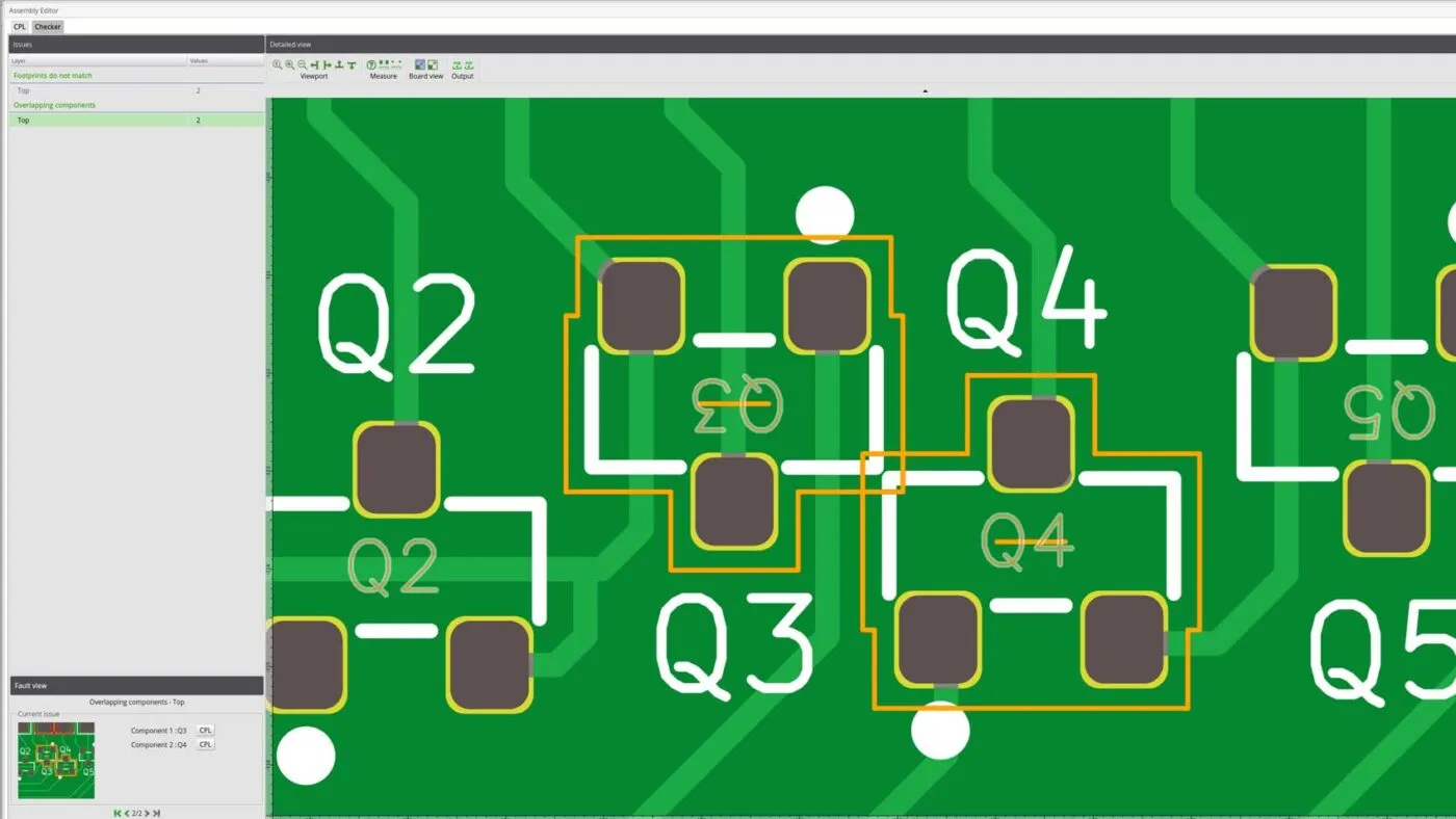
The Importance of Courtyard Areas: Preventing Assembly Mishaps in PCB Design
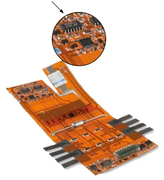
Troubleshooting Common Issues in Flex-to-Install PCB Assembly
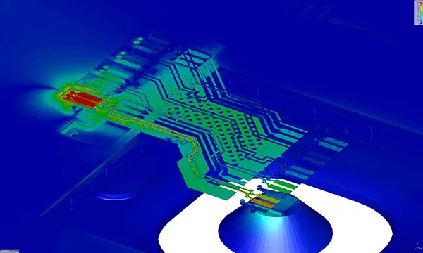
The Impact of Design for Repairability on PCB Lifespan and Cost
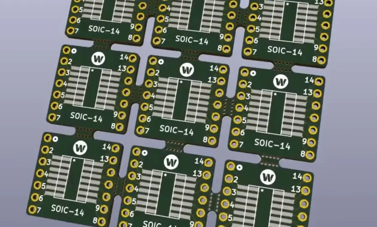
PCB Panel Size and Component Placement: Best Practices