 00:55
00:55
HDI PCB Stackup
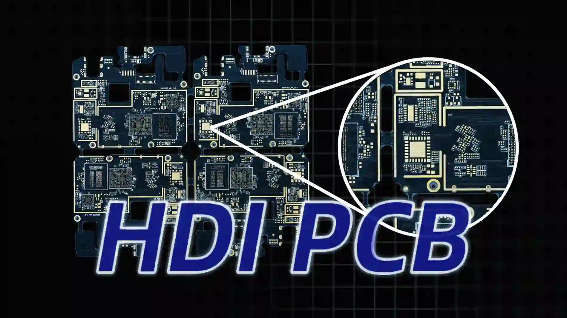
High-density interconnect (HDI) PCB stackup is a critical aspect of modern electronics design, enabling the creation of compact, high-performance circuit boards that support advanced functionalities in devices like smartphones, medical equipment, and automotive systems. At its core, HDI PCB stackup refers to the layered arrangement of conductive and insulating materials in a printed circuit board, incorporating fine-pitch features such as microvias, buried vias, and sequential lamination to achieve higher component density and improved signal integrity. For engineers and designers searching for HDI PCB stackup solutions, this tag serves as a comprehensive resource, offering insights into optimizing board layouts for space-constrained applications while minimizing electromagnetic interference and thermal issues. Understanding the nuances of HDI PCB stackup can significantly enhance design efficiency. Key considerations include selecting the appropriate number of layers—typically ranging from 4 to 12 or more—based on signal routing requirements and power distribution needs. Best practices involve using laser-drilled microvias for precise interconnections between layers, which reduce via stubs and improve high-speed performance. Practical applications extend to industries where miniaturization is paramount, such as wearable technology and IoT devices, where a well-designed stackup can lower manufacturing costs by reducing board size and material usage. Designers often benefit from simulation tools to predict impedance control and crosstalk, ensuring reliable operation in real-world scenarios. This collection of articles delves into various HDI PCB stackup configurations, from standard 1+N+1 builds to more complex any-layer designs, providing step-by-step guidance on implementation. Whether you're troubleshooting common pitfalls like layer misalignment or exploring innovative materials like high-Tg laminates for better heat resistance, the content here equips you with actionable strategies to refine your projects. Browsing through these resources can help you stay updated on evolving standards and techniques, fostering more robust and efficient PCB designs.
Video Guide

Technical Articles

Overview of PLC Ethernet Open Communication
End-to-End Autonomous Driving Perception: PCB Design Challenges for BEV, 3D Detection, and High-Performance AI Architectures
HDI Multilayer PCB Design: Advanced Techniques for High-Density Boards
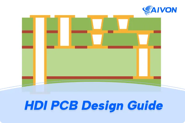
HDI Design Guide: Stackup Principles, Microvia Reliability and High-Density Routing Guide
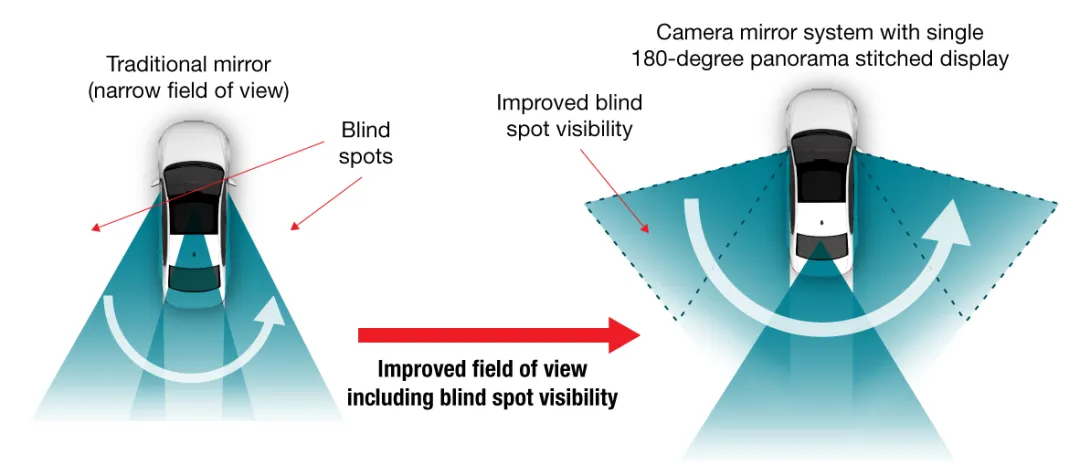
Digital Cockpit Systems: High-Performance PCB Design for Automotive SoC Integration, Multi-Display, and In-Cabin Sensing
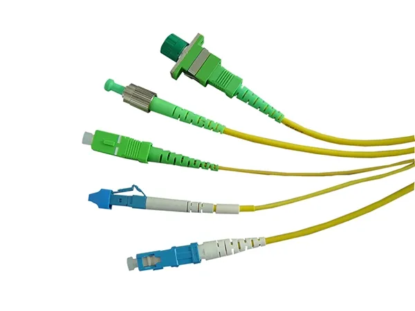
Advanced PCB Design Strategies for Fiber Optic Modules and LiFi Wireless Communication Systems

Overview of Network Security Devices: PCB Design, Manufacturing, and Reliability Considerations
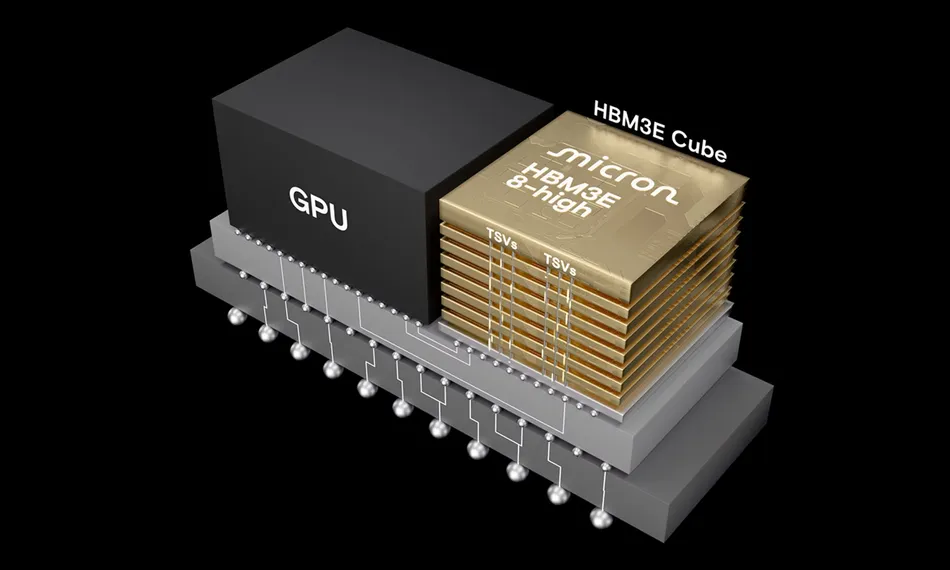
Comparing HBM, HBM2, HBM3 and HBM3e
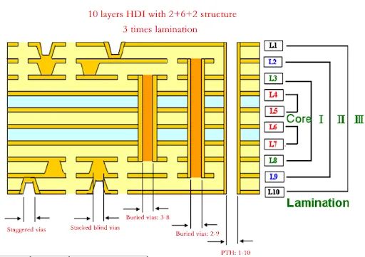
Via Aspect Ratio in PCB Design: Considerations for HDI Complex PCBs
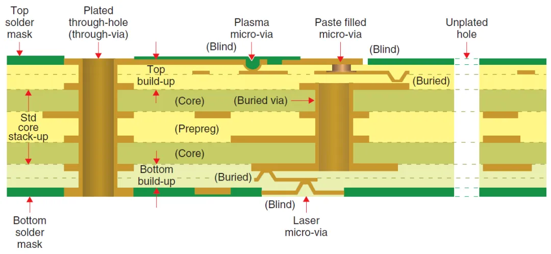
Microvia Aspect Ratio: Achieving High Density Interconnects
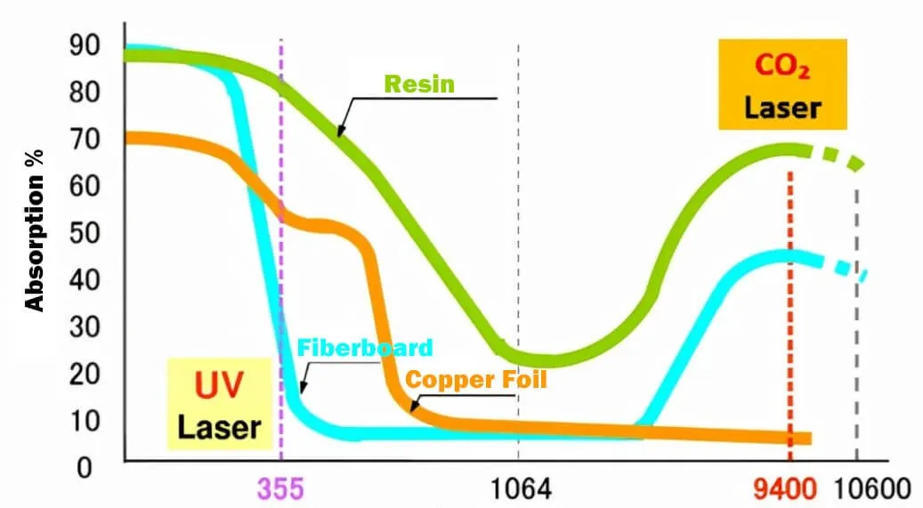
HDI PCB Laser Drilling: Materials, Techniques, and Equipment
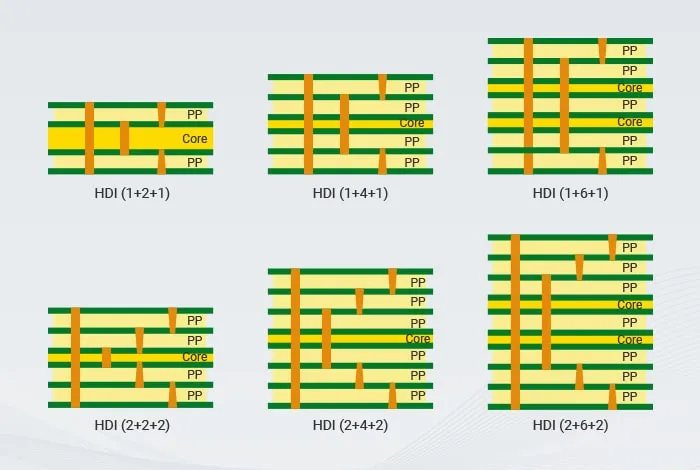
HDI PCB Stack Up Design: Optimizing Layer Count and Signal Routing

Cellular Mobile Technology: PCB Design and Manufacturing for 4G/5G Networks
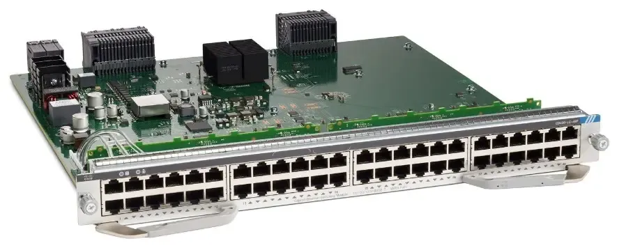
Designing an HDI Network Switch PCB for High-Speed, High-Density Networking
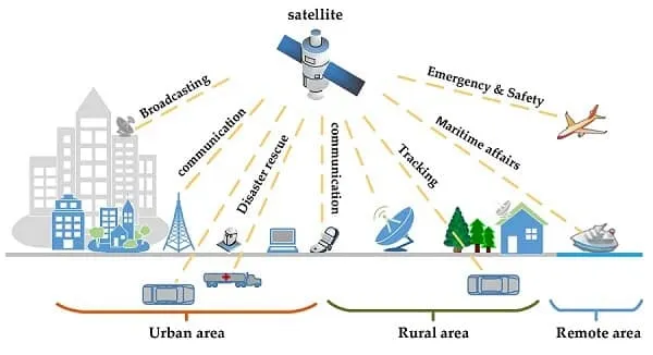
PCB Design and Manufacturing Strategies for Satellite Internet and NTN Voice Systems
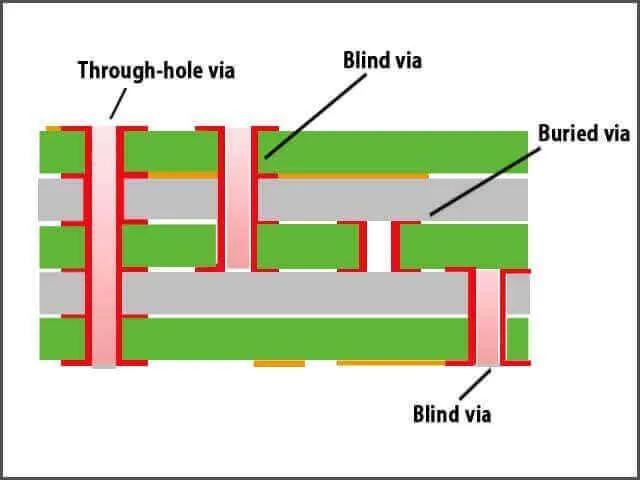
Blind Vias in PCB Design: Optimizing High-Density Boards
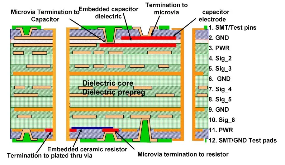
HDI Assembly: Stack Up Structures and Materials
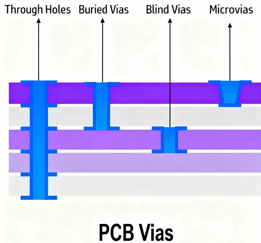
Stacked Vias in HDI PCBs: Design, Manufacturing, and Reliability
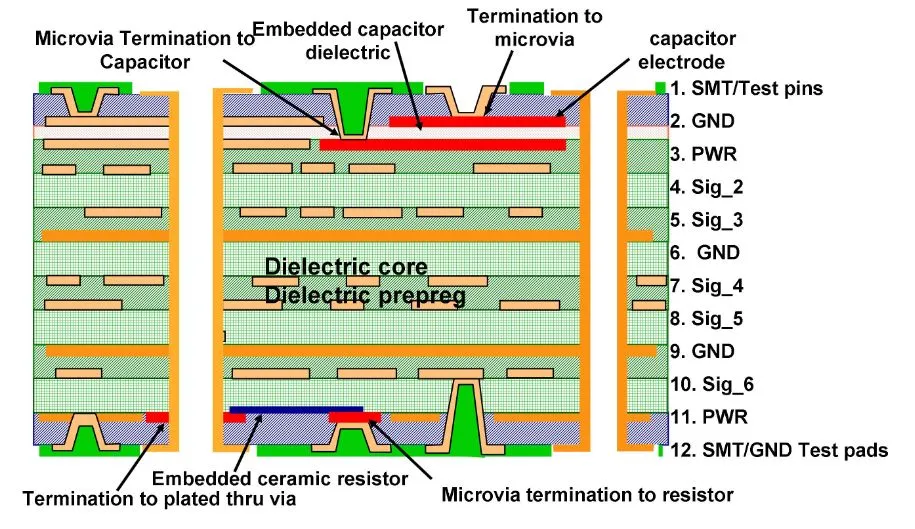
Advanced HDI PCB Stackup Materials for Improved Signal Performance