Impedance Matching
Impedance matching is a fundamental concept in electronics and PCB design that ensures optimal signal transmission and power transfer between components or systems. By aligning the impedance of a source with that of its load, engineers can minimize reflections, reduce signal distortion, and enhance overall circuit performance. This technique is particularly crucial in high-frequency applications, such as RF circuits, telecommunications, and high-speed digital systems, where mismatches can lead to significant energy loss or data errors. For professionals and hobbyists searching for impedance matching resources, this tag page serves as a centralized hub for articles that delve into practical strategies and real-world implementations. You'll find guidance on calculating characteristic impedance in transmission lines, selecting appropriate matching networks like L-sections or pi-networks, and integrating these into PCB layouts to maintain signal integrity. Best practices include using tools like Smith charts for visualization, simulating designs with software such as LTSpice or ADS, and considering factors like trace width, dielectric materials, and via configurations to achieve precise matching. Understanding impedance matching not only helps in troubleshooting common issues like standing wave ratios (SWR) but also empowers designers to build more efficient systems, from antennas to amplifiers. Whether you're optimizing a microwave circuit or ensuring reliable data rates in Ethernet interfaces, these insights provide actionable steps to elevate your projects. Browse the linked articles below to explore specific case studies, tutorials, and advanced techniques tailored to various electronics challenges.
Technical Articles
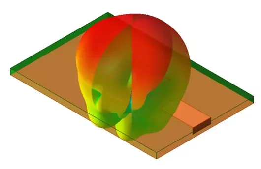
How Antennas Work and Why They Vary
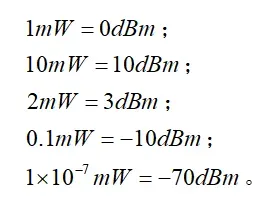
Basic Units in RF: dB, dBm, and dBW
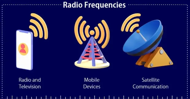
RF PCB Design Essentials: Radio Frequency Principles for High-Performance Wireless Systems
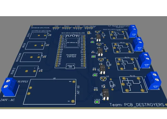
Signal Integrity Challenges in High Speed Smart Home Device PCBs
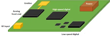
PCB RF Antenna Design and Layout: Engineering Principles, Isolation Techniques, and Manufacturing Integration
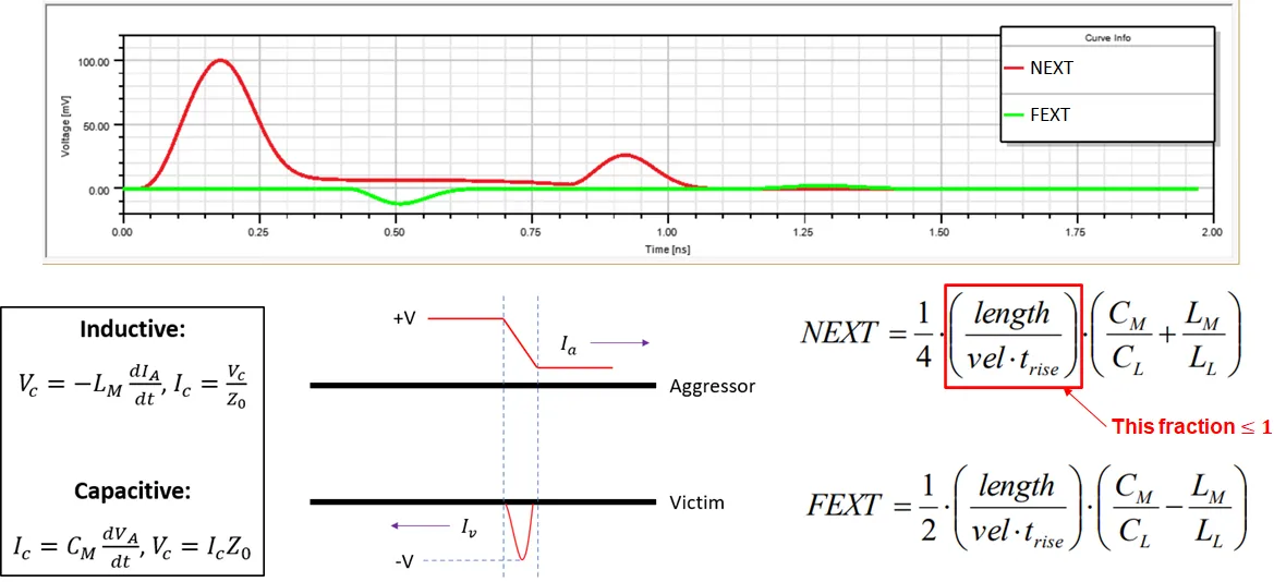
Mastering Impedance Matching in PCB Design for Optimal Signal Integrity
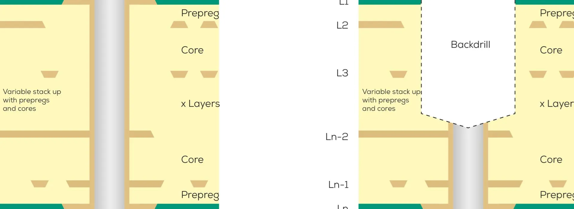
The Impact of Controlled Depth Drilling on High Speed PCB Performance
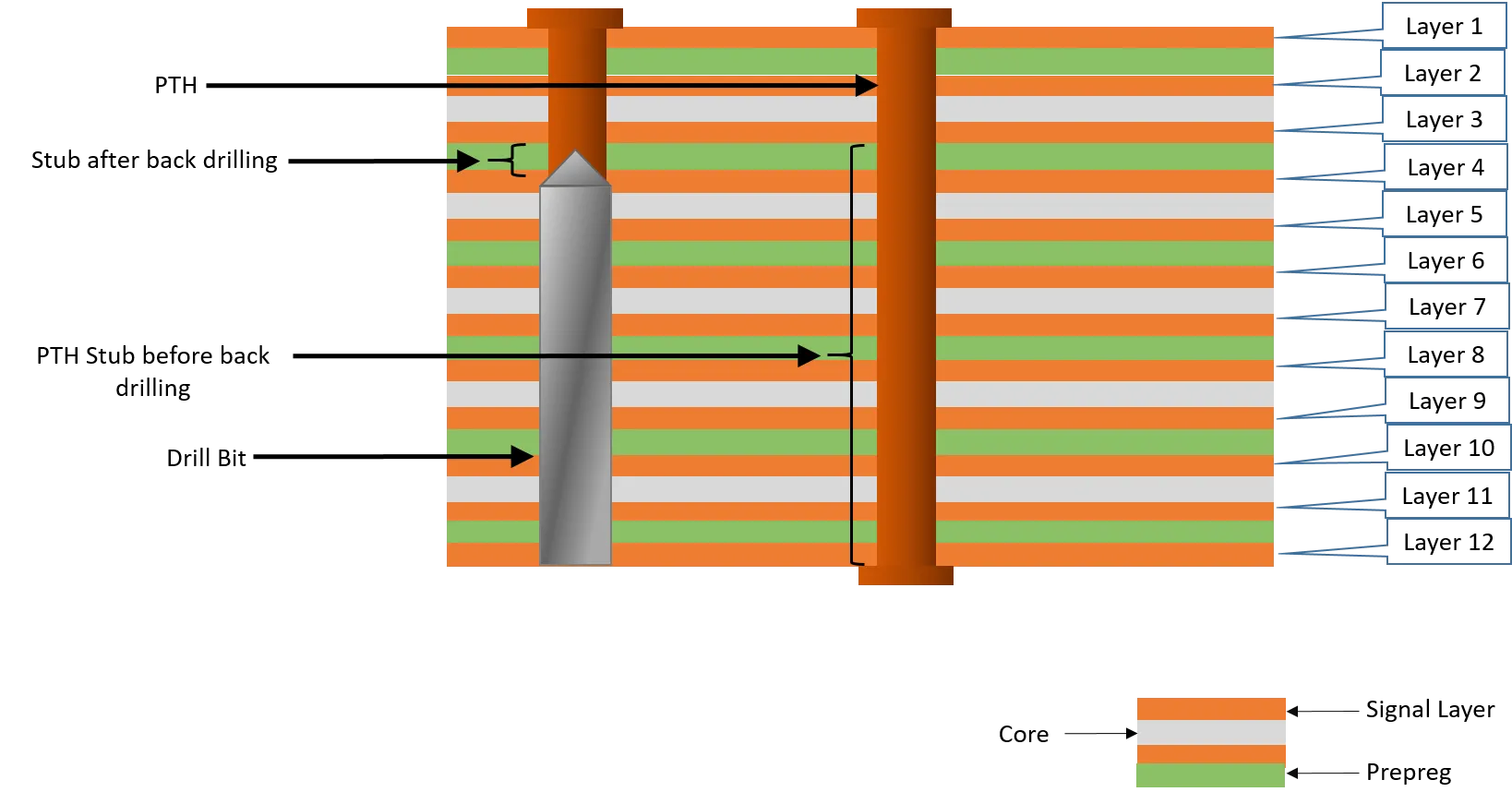
The Role of Controlled Depth Drilling in RF PCB Design
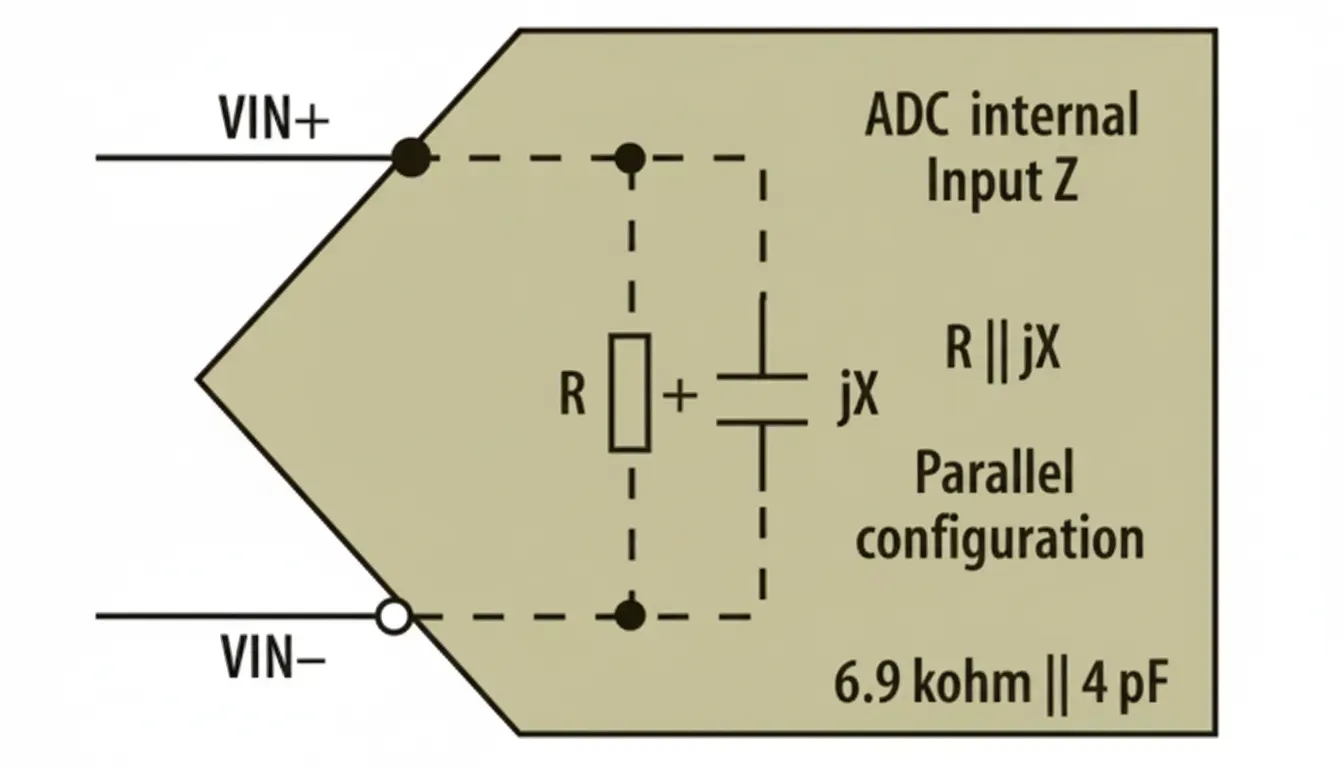
Five Practical Steps to Design an ADC Front-End
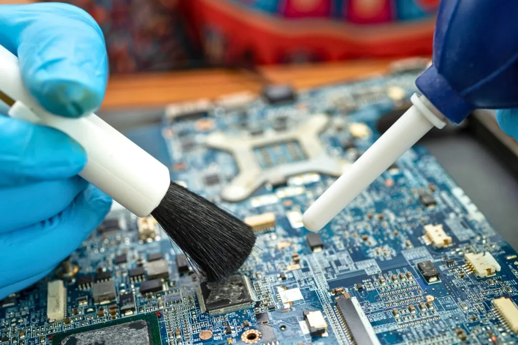
PCB Cleaning for High-Frequency Applications: Minimizing Signal Loss and Maximizing Performance
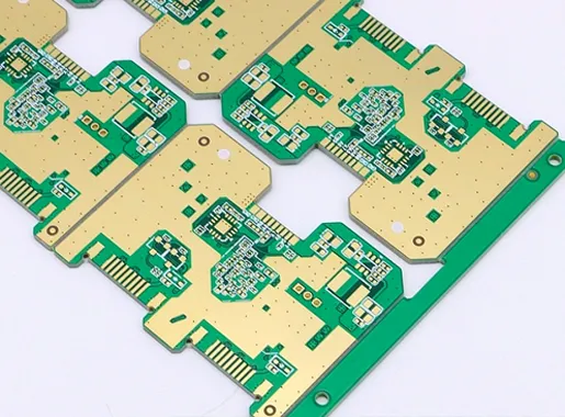
The Impact of Halogen Free PCBs on Signal Integrity: What Engineers Need to Know
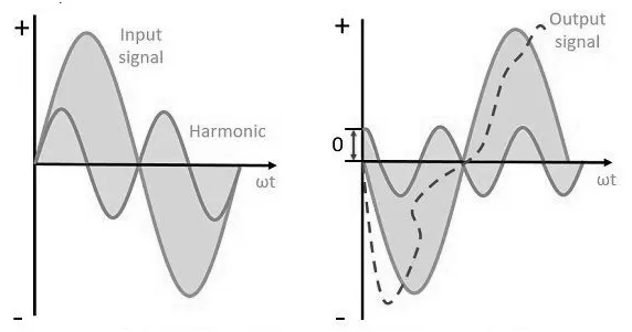
Types of Amplifier Distortion and How to Reduce Them
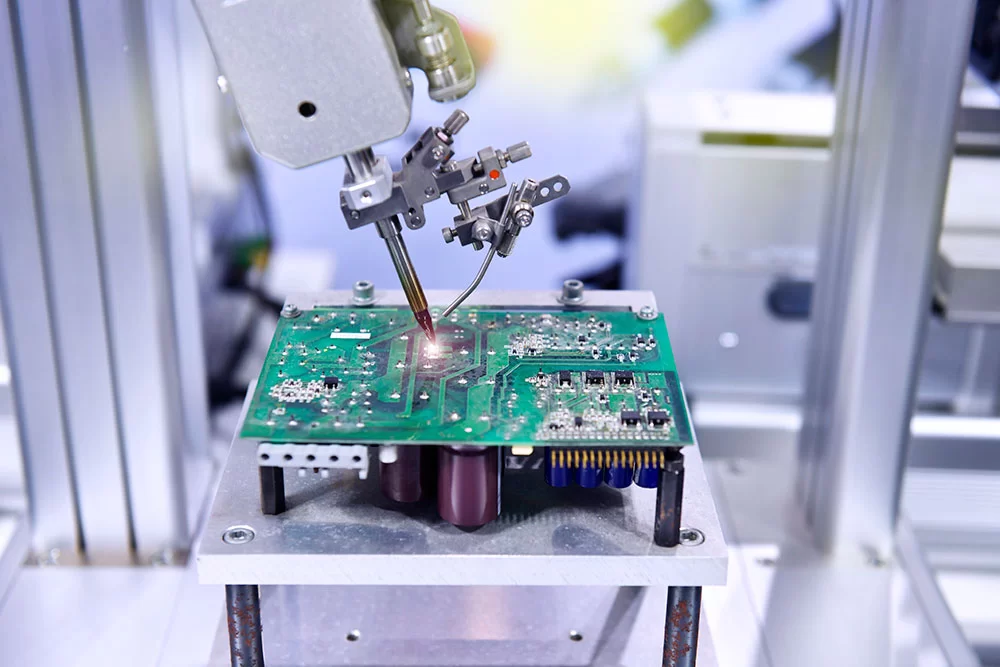
Microvia PCB for RF Applications: Design Considerations for High Frequency Performance
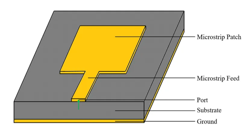
High Frequency PCB Layout Techniques for Satellite Communication Systems

Router PCB Design for Beginners: A Step-by-Step Guide to Networking Hardware
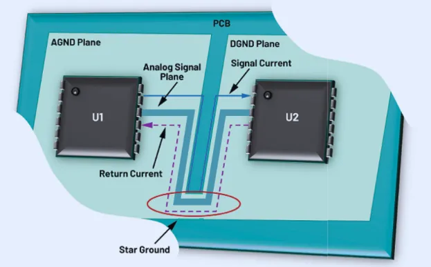
Mastering PCB Signal Routing for Crystal-Clear Audio Amplifiers
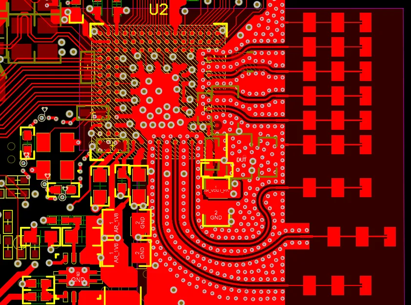
RF PCB Design Guidelines: Key Principles and Best Practices

Fan Microstrip Structures in RF Amplifiers