 00:47
00:47
PCB Stackup Design
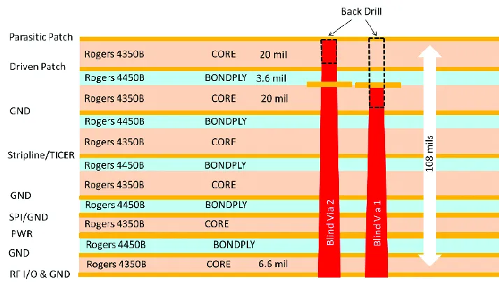
PCB stackup design is a fundamental aspect of printed circuit board engineering that determines the arrangement of conductive and insulating layers within a PCB. This configuration plays a critical role in ensuring signal integrity, managing electromagnetic interference, and optimizing thermal performance in electronic devices. For engineers and designers searching for insights on PCB stackup design, this tag aggregates resources that delve into the principles and methodologies for creating effective multilayer boards, from simple two-layer setups to complex high-speed applications. Understanding PCB stackup design begins with selecting appropriate layer counts, materials, and via structures to meet specific project requirements. Key considerations include controlled impedance for high-frequency signals, power distribution planes to minimize noise, and ground layers for shielding. Practical applications span industries such as telecommunications, automotive electronics, and consumer gadgets, where poor stackup can lead to issues like crosstalk or signal degradation. Best practices emphasize simulation tools for pre-layout analysis, adherence to manufacturing constraints, and iterative testing to refine designs, ultimately reducing prototyping costs and time to market. Articles under this tag offer detailed guides on topics like symmetric versus asymmetric stackups, the impact of dielectric constants on performance, and strategies for high-density interconnects. Whether you are troubleshooting a current project or planning a new one, these resources provide actionable steps to enhance your PCB designs. Dive into the collection to find case studies, tutorials, and expert tips that align with real-world challenges in electronics development.
Video Guide

Technical Articles
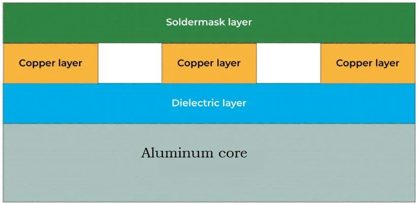
A Beginner's Guide to Metal Core PCB Stackup Design
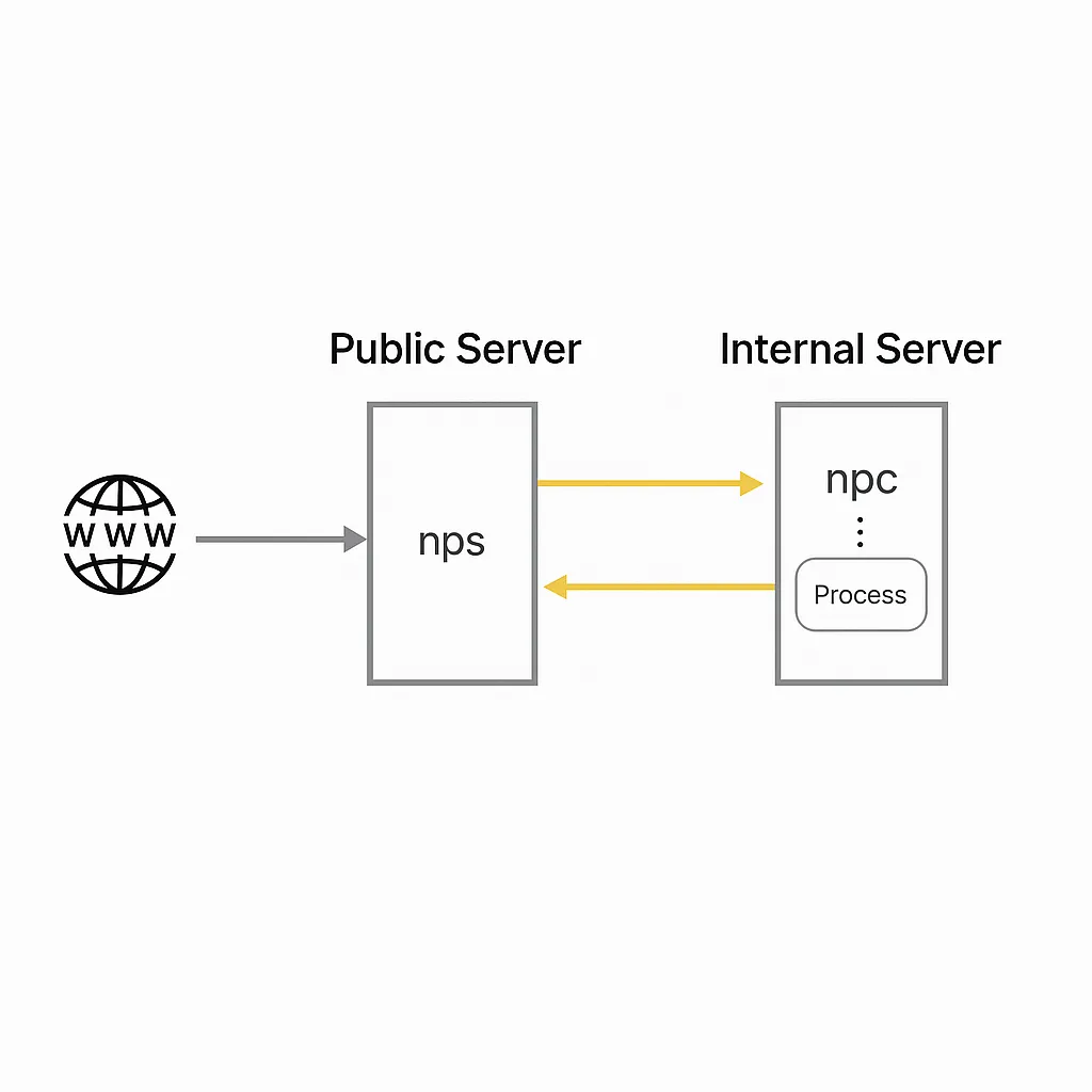
Common NAT Traversal Tools: Principles and Usage

First Phones with Snapdragon 8 Gen3
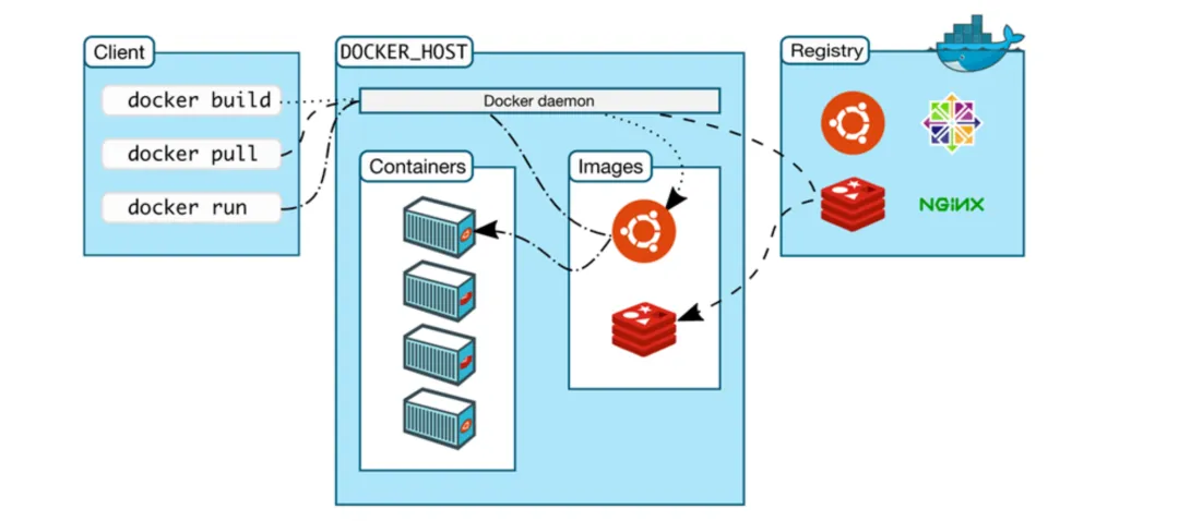
How Cloud Security Differs from Traditional Security
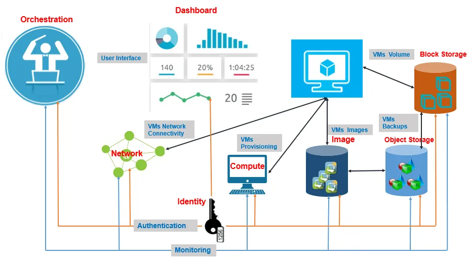
OpenStack Network Models and Use Cases
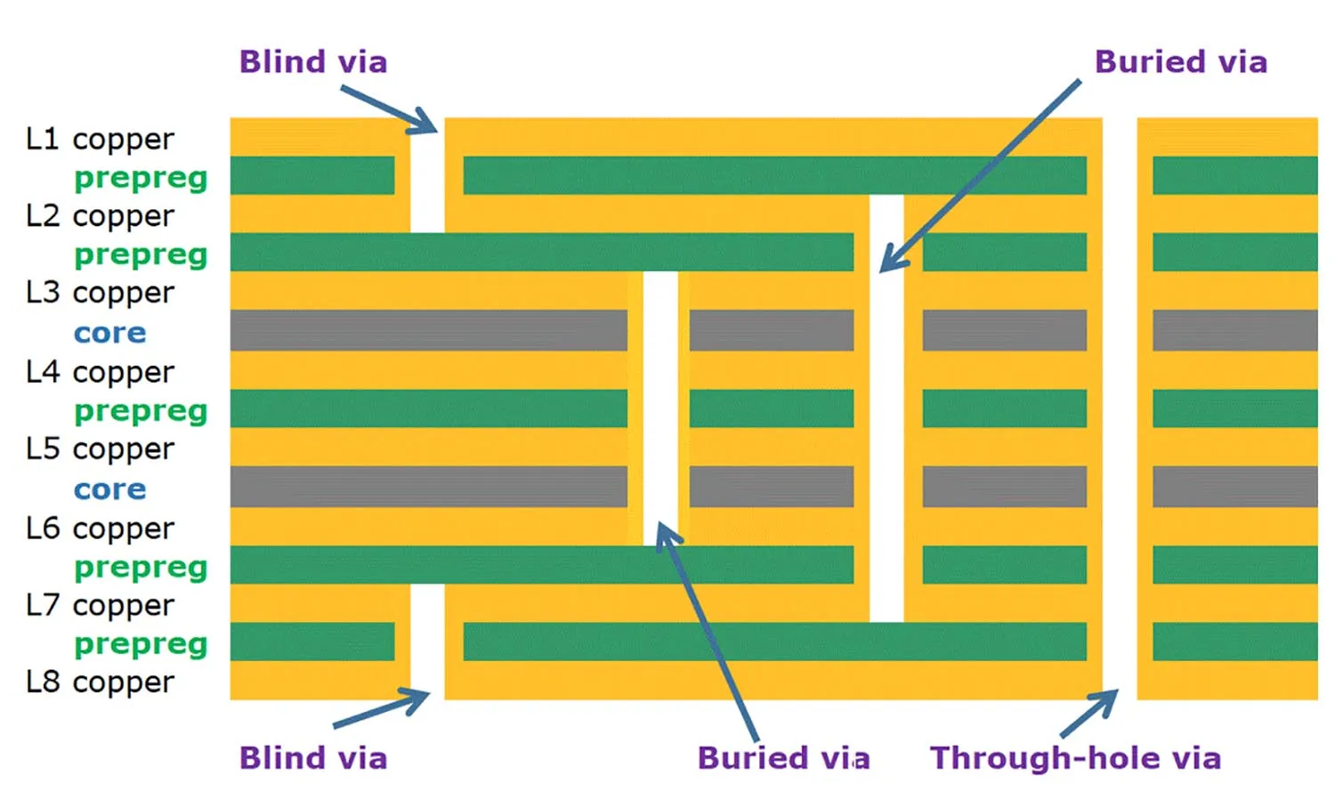
Optimizing PCB Stack Up for High Speed Signals: A Comprehensive Guide
Optimizing PCB Stack Up for RF Applications: A Practical Guide
ZHITAI Ti600 QLC SSD Review: Performance, Reliability, and PCB Integration Insights
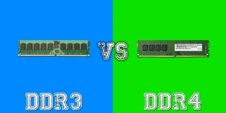
DDR3 vs DDR4: Technical Characteristics Compared
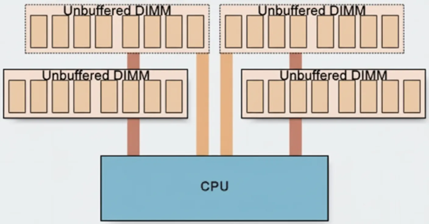
DDR3 and DDR4 Memory: Technical Notes
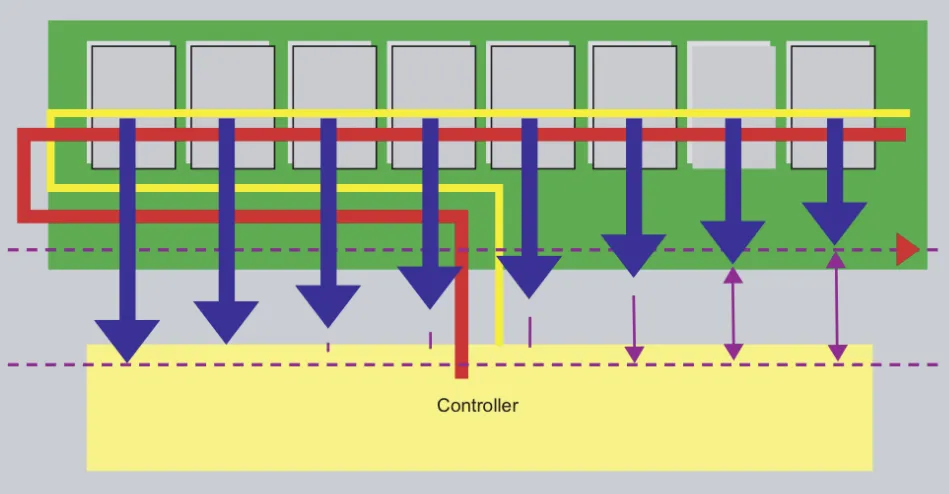
DDR3 Bandwidth Calculation
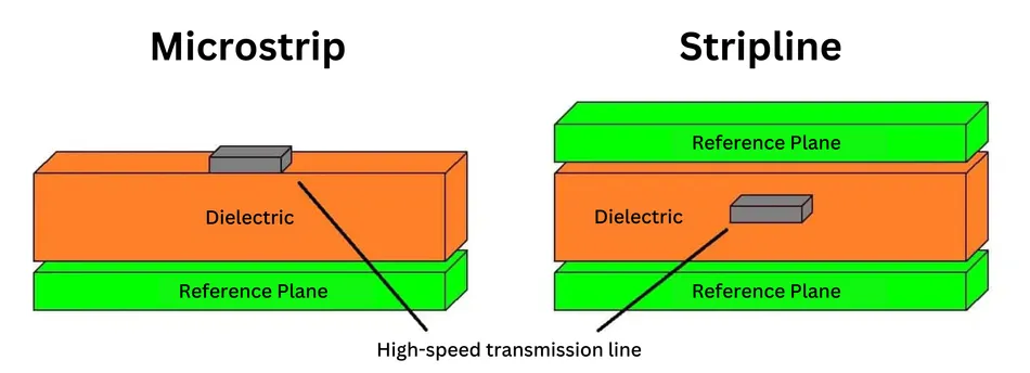
Advanced PCB Impedance Control: Techniques for Minimizing Signal Loss

How Do Smartphones Determine Location?
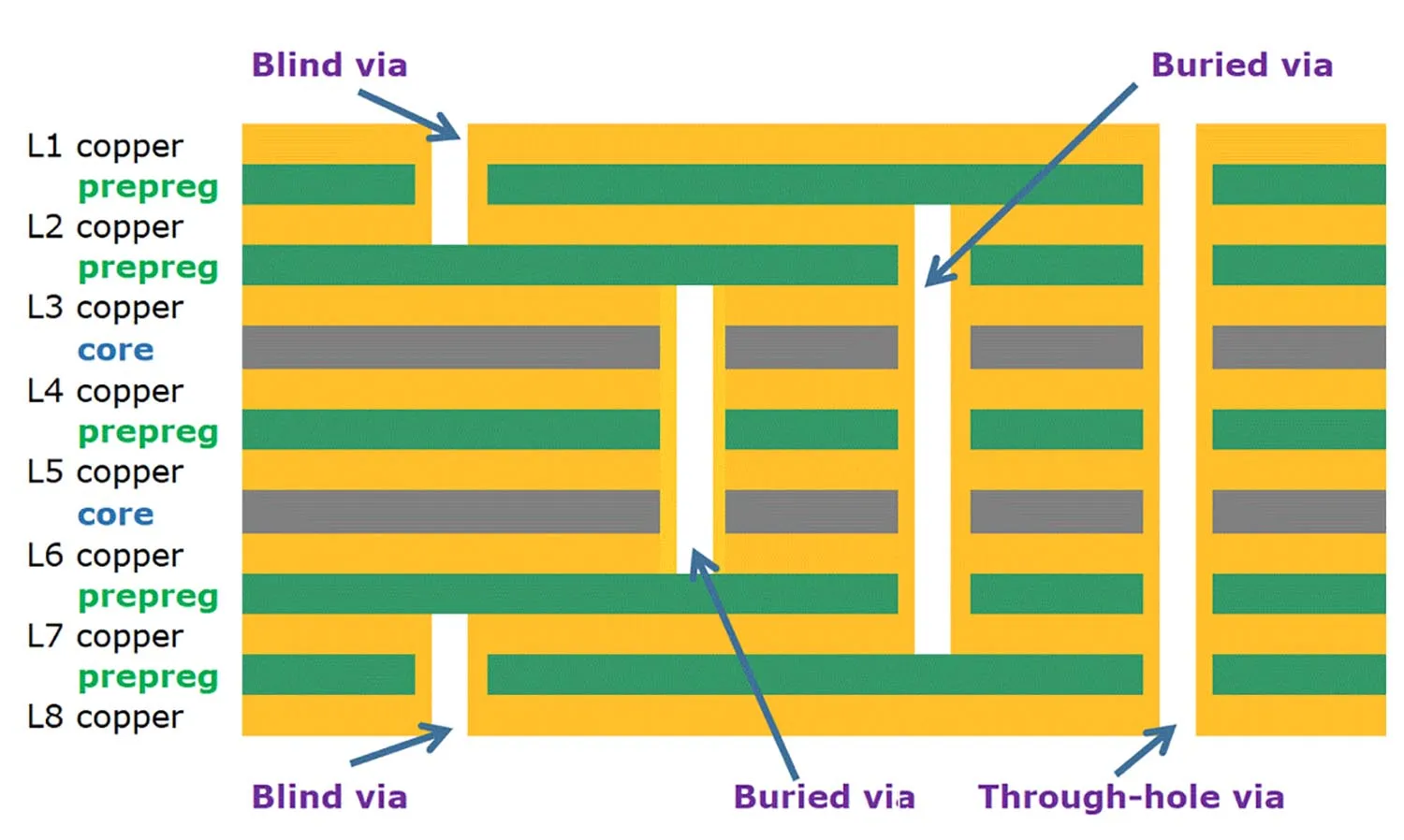
Impedance Controlled PCB Manufacturing: Overcoming Challenges in Design and Fabrication
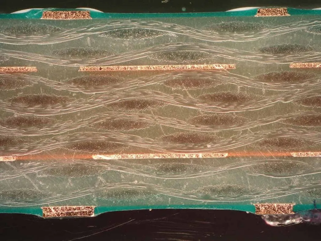
High Tg PCB Manufacturing: Design Tips for Optimal Performance

What Is 5.5G and How It Differs from 5G and 6G
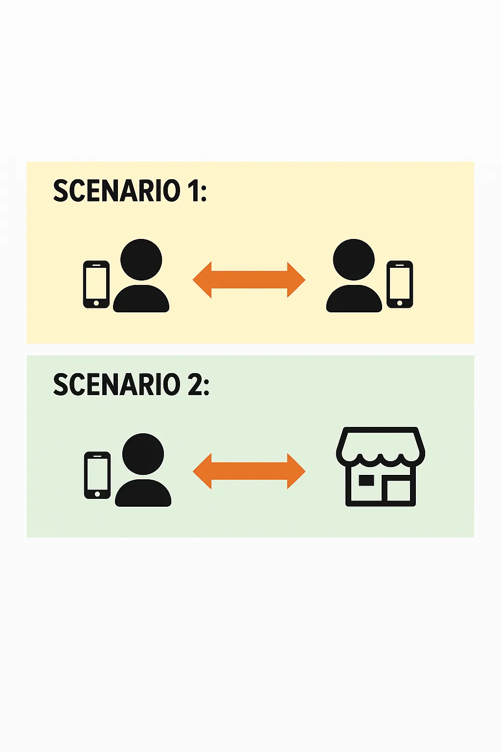
What Is 5G Messaging and Why Is It Being Promoted?

Key Parameters of Next-Generation Firewalls

VoNR Solution for 5G Networks