










Solder Joint Reliability
Solder joint reliability is a critical aspect of printed circuit board (PCB) design and manufacturing, focusing on the long-term performance and durability of connections between components and the board. In electronics, solder joints serve as the backbone of electrical and mechanical integrity, but they can degrade over time due to factors such as thermal expansion, mechanical vibration, humidity, and material fatigue. For engineers, technicians, and hobbyists searching for information on this topic, understanding solder joint reliability helps prevent common failures in consumer devices, automotive systems, industrial equipment, and aerospace applications. By addressing these challenges early in the design phase, professionals can enhance product lifespan and reduce costly rework or recalls. This tag encompasses a range of articles that delve into the science behind solder joint failures, including intermetallic compound formation, voiding, and cracking under stress. Readers will find practical guidance on selecting appropriate solder alloys, such as lead-free options compliant with RoHS standards, and optimizing reflow soldering processes to minimize defects. Best practices include implementing accelerated life testing methods like thermal cycling and shear testing to predict real-world performance, as well as using advanced inspection tools such as X-ray imaging or cross-sectional analysis for quality assurance. These insights are particularly valuable for those troubleshooting field failures or seeking to comply with industry standards like IPC-9701 for reliability assessment. For deeper knowledge, the articles linked under this tag offer case studies from real-world scenarios, step-by-step tutorials on improving joint strength through design modifications, and comparisons of soldering techniques like wave versus reflow. Whether you are refining prototypes or scaling production, these resources provide the technical foundation to achieve robust, reliable solder joints that withstand demanding environments.
Technical Articles

Can a 0 Ω Resistor Really Be Used as a Jumper? A Trap Many Engineers Have Hit
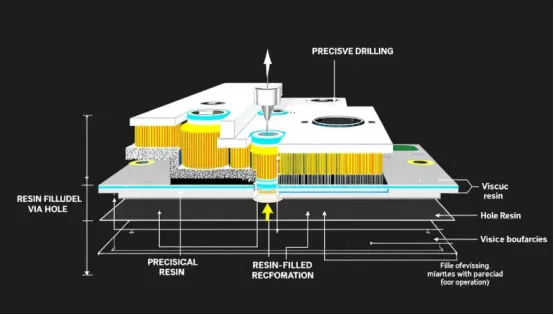
Which Vias Need Resin Plugging? Real Engineer Questions from Production
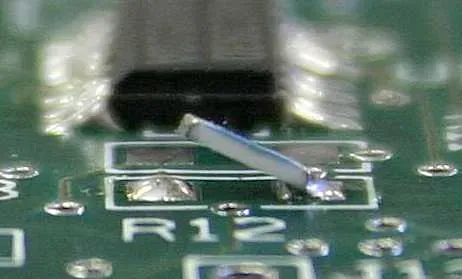
Can a Via Be Placed in a Pad? A Detail PCB Designers Cannot Skip

Why Traces Can Still Open After Teardrops Are Added to Vias
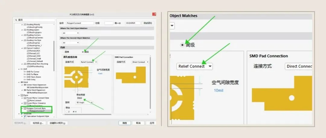
Why Does a Pad Tied Straight to a Copper Pour Become More Prone to Poor Soldering?
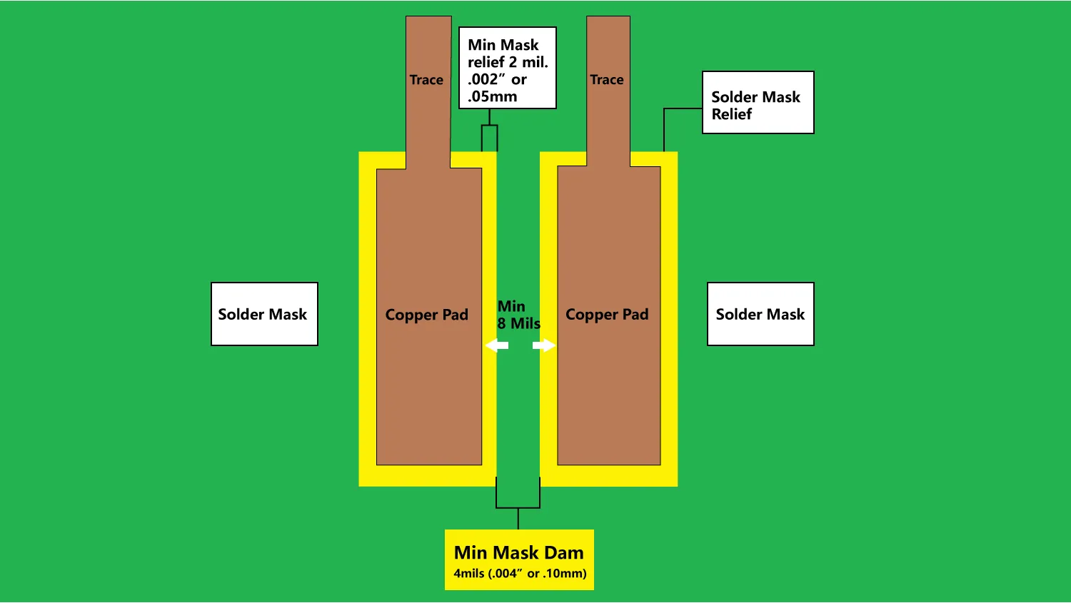
Why Your Solder Mask Bridge Keeps Failing – Real Spacing Limits from Production
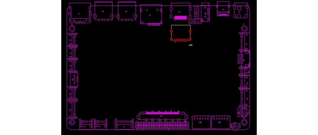
Why a Small Shift in Footprint Origin Moves Every Pick-and-Place Coordinate
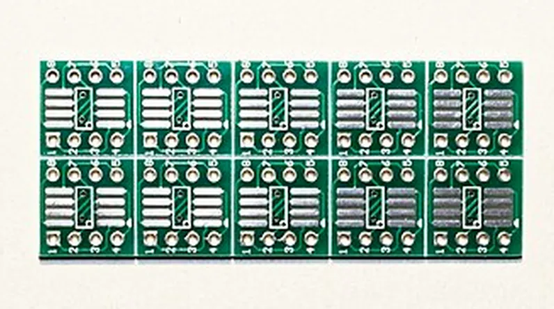
Why Do Copper Traces Near V-CUT Edges Crack During Depaneling?

Interpreting IPC-7801: Process Control Standard for SMT Reflow Soldering

Analysis of 20 Common Defects in Wave Soldering and Their Causes

What Is Cpk (Process Capability Index)?

Reflow Technologies for Reducing Solder Voids

Root Cause Analysis and Control of the Galvanic Effect in PCB Immersion Silver

Applying Fishbone Diagram Analysis to SMT Process Defects

Why Components Must Be Kept Away from PCB Edges: Understanding SMT Rail Keep-Out Zones

Why Must You Pass Through an Air Shower Before Entering an SMT Workshop?

Compatible Pad Design and Soldering Reliability Validation for FCQFN and WLCSP Packages

Lead-Free Alloy Reflow Temperature Profiles and Analysis of Soldering Defects


