










KiCad Hub
KiCad Hub: Guides, Tips, and Best Practices
Featured Blog
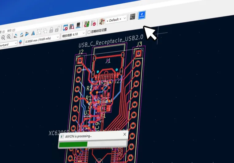
How to Install and Use AIVON KiCad Plugin for PCB Ordering
Step-by-step guide to install the AIVON KiCad plugin, get instant PCB quotes, and skip manual Gerber uploads. Learn the complete workflow from design to manufacturing.


Latest Blogs
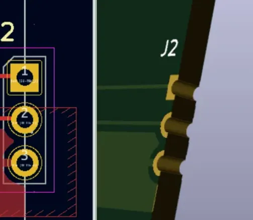
Designing PCB Castellated Holes with KiCad
Design PCB castellated holes in KiCad, configure DRC using the Castellated (THT only) pad attribute, and address manufacturing and assembly considerations.

Defining and Using Differential Pairs in KiCad
KiCad differential pair routing: net naming (P/N, +/-), Board Setup constraints (width, gap, via gap), via pairs, net classes/regex rules, and current limitations.
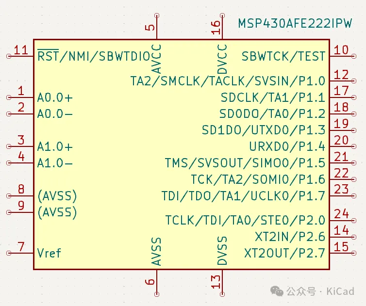
Using Alternate Pins in KiCad
Learn how to define and select alternate pin functions in KiCad to capture multiplexed MCU pins clearly, improve schematic readability, and generate meaningful netlists.

Adding Via Stitching in KiCad with the kicad-action-scripts Plugin
Learn how to add via stitching in KiCad using the kicad-action-scripts plugin. Installation, configuration, editing, limitations, and best practices for EMI, return paths, and thermal.
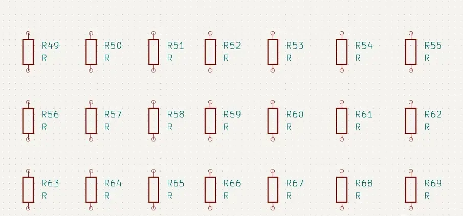
How to Continuously Place the Same Symbol in a KiCad Schematic
Enable continuous symbol placement in KiCad with the Place copies option and speed up schematic capture using the Insert shortcut for auto-incremented net labels and duplicated wire segments.

Do Gerber File Extensions Have Any Special Meaning?
Learn how Gerber file extensions are used across EDA tools, what Altium/Protel suffixes mean, how Gerber X2 embeds layer attributes, and when to consider ODB++ or IPC?2581 for clearer PCB fabrication data.

Do You Need a Full-Board Copper Pour on Your PCB?
Should your PCB use a full-board copper pour? Learn how pours control return paths, reduce loop inductance, improve EMI, and when they’re essential for high-speed designs.
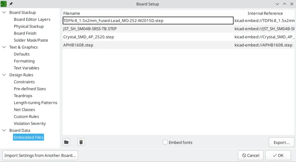
File Embedding Explained (Part 1): Embedding 3D Models in PCB Footprints
Learn how KiCad 9 embeds STEP 3D models directly in footprints or PCB files using kicad-embed references and StepZ compression, improving portability and reducing broken links while managing file size.
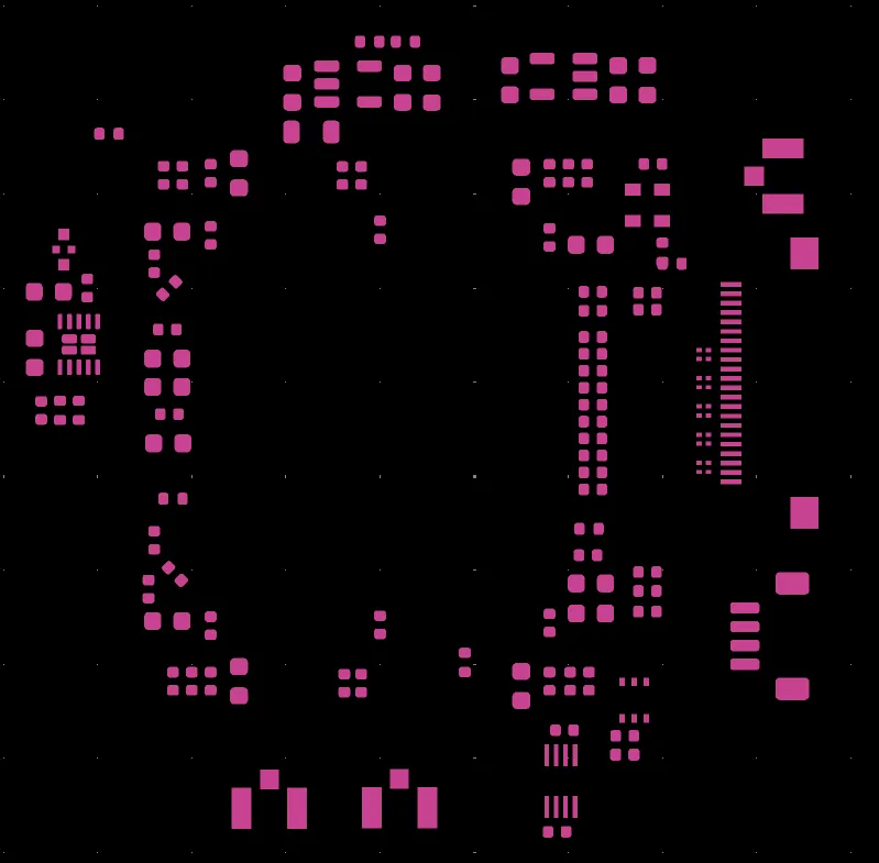
What Are Adhesive Layers in KiCad PCB? A Practical Guide to Red Glue in SMT
Learn how KiCad’s F.Adhesive and B.Adhesive layers map to SMT manufacturing, what the red glue process is, when to use it, application methods, and how it compares with solder paste and mechanical fixtures.

Mastering KiCad 3D Models: Linking Footprints, Embedding Files, Ray Tracing, and CLI Exports
Learn how to find and link 3D models in KiCad, align and embed them in footprints, enable ray tracing for photorealistic renders, and automate STEP exports via the CLI for robust ECAD–MCAD workflows.
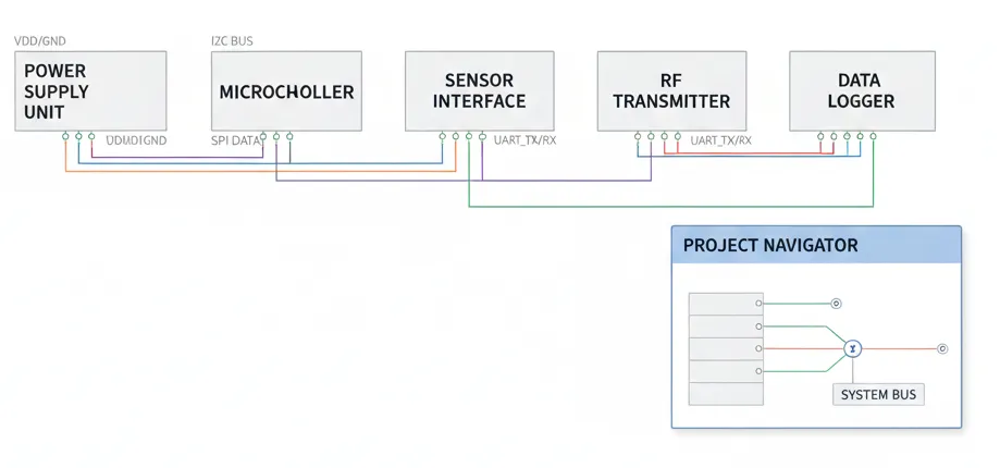
KiCad Finally Supports Flat (Tiled) Schematic Structure!
KiCad 9.99 nightly previews flat (tiled) schematics: adds multiple top-level pages and UI controls for managing them. Backup files—9.99 format differs from 9.0.x.
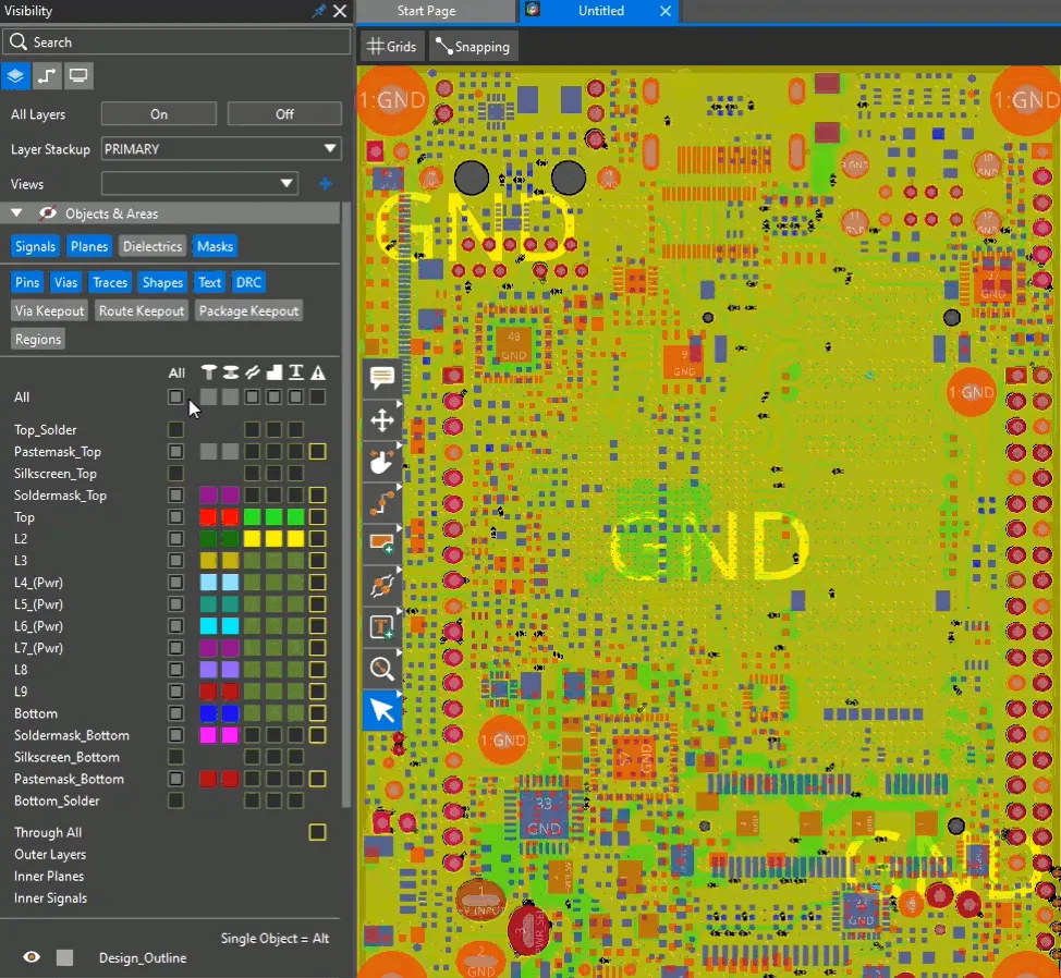
From Altium to Allegro: Which EDA Formats Can KiCad Import?
Survey of KiCad 10 import capabilities for third?party EDA formats: supported schematic and PCB types, stable vs development importers, and practical migration checks.


