


PCB Assembly
Printed circuit board (PCB) assembly represents a critical phase in electronics manufacturing, where components are mounted onto a board to create functional circuits. This process bridges design and production, ensuring that electronic devices perform reliably in diverse applications. From soldering techniques to component placement, PCB assembly encompasses the methods and technologies that transform bare boards into operational systems. Understanding these elements is essential for engineers, hobbyists, and industry professionals aiming to optimize production efficiency and product quality. Within this category, readers will find a comprehensive collection of guides that detail step-by-step assembly processes, tutorials on advanced tools like surface-mount technology and automated pick-and-place machines, and insights into troubleshooting common issues such as solder joint defects or thermal management challenges. Best practices are highlighted to promote reliability, including strategies for minimizing defects through quality control measures and adhering to industry standards like IPC guidelines. These resources draw from real-world expertise to address both fundamental concepts and cutting-edge innovations in the field. The practical value of mastering PCB assembly extends to numerous sectors, including consumer electronics, automotive systems, medical devices, and aerospace engineering. By applying the knowledge shared here, professionals can reduce manufacturing costs, accelerate time-to-market, and enhance device durability. For instance, effective assembly techniques ensure that circuits withstand environmental stresses, leading to longer-lasting products in demanding conditions. Delving into the articles in this PCB assembly category provides a pathway to deeper technical proficiency. Whether refining prototyping skills or scaling up production, the content equips readers with actionable strategies to tackle real-world challenges and stay ahead in an evolving industry.
Latest Blogs

Wave Soldering in Through-Hole Assembly: Practical DOE Case Studies for Yield Improvement
Wave soldering DOE identifies factors for PTH solderability, defines thermal relief guidelines, and optimizes flux, preheat, conveyor angle, and contact time.

SMT Solder Paste Printing Process: Analysis and Practical Optimization
SMT solder paste printing guide on alloy/flux selection, stencil design, process windows, defect root-cause analysis, and SPI closed-loop control to improve first-pass yield.

Root Cause Analysis and Corrective Actions for a 76% Open-Solder Rate on Recycled BGA Devices
Root cause analysis of high open solder joints on reclaimed CPU BGA; X-ray shows BGA warpage; press block mitigation restored reliable joints.

Dye Stain Analysis of SMT BGA Defects: A Review of Five Typical Cases
Five SMT BGA failure-analysis cases using the dye stain method, covering corner cracks, reflow-induced voiding, mechanical stress near standoffs, and verification practices.
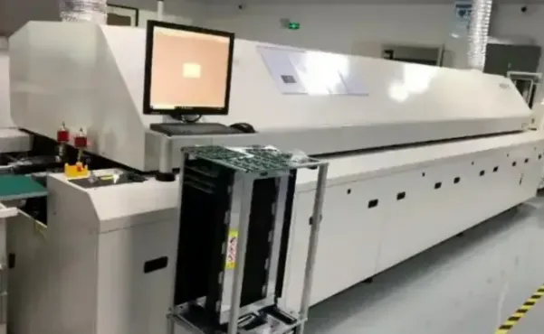
IPC-7801: Process Control for SMT Reflow Soldering
Technical overview of IPC-7801 process control for SMT reflow soldering, detailing thermal profiles, conveyor speed, atmosphere, inspection, and calibration.
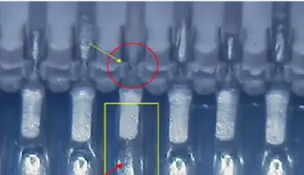
Root Cause and Corrective Action for CF Card Connector Solder Opens in SMT
Case study of CF Card SMT connector solder opens: coplanarity loss at middle pins diagnosed; fixed with deeper thermal staking; verified at 100% yield.

BGA Soldering Defects: A Comprehensive Guide for SMT Process Engineers
BGA reflow defects explained: detection via X-ray/borescope, root causes, and process fixes for solder bridging, cold joints, opens, warpage, and head-in-pillow.
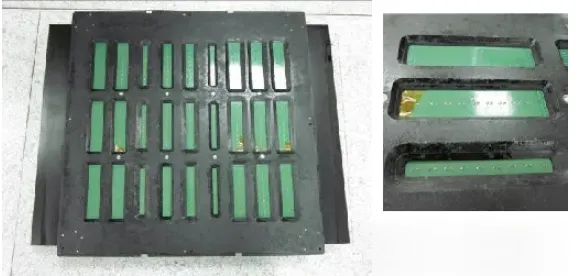
Improving DIP Solder Fill: A DOE on Thermal Relief Pads and PTH Clearance
DOE on DIP wave soldering identifies key drivers of hole fill: PTH clearance and carrier aperture; with thermal relief design guidance.
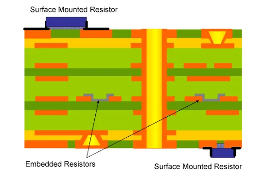
20-Layer Embedded-Resistor PCB: Process Flow and Core Manufacturing Challenges
Engineering guide to a 20-layer embedded-resistor PCB, focusing on multi-stage lamination, with controls for via fill planarity, depth accuracy, and stack-wide impedance.
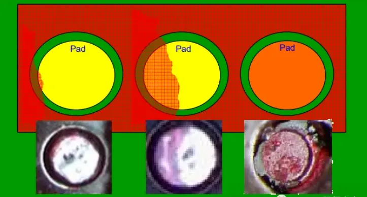
SMT BGA Failure Analysis by Dye Stain: Procedure, Criteria, and Practical Cases
Technical guide to BGA solder joint dye-and-pry analysis: materials, workflow, precautions, void acceptance criteria, crack classification, and cross-section evaluation.

Common Process Challenges in SMT Reflow Soldering
Survey-backed analysis of SMT reflow soldering defects and process control, focusing on temperature profiling, oven stability, airflow, cooling, and reliability.

Root Causes of PCB Expansion and Shrinkage and How to Mitigate Them
Technical analysis of PCB dimensional change across cutting, imaging, lamination, laser, via fill, and solder mask, with metrology controls and SMT reflow mitigation.


