










PCB Knowledge
Printed circuit boards (PCBs) form the backbone of modern electronics, enabling everything from smartphones to industrial machinery. In our PCB Knowledge category, we delve into the essential principles, techniques, and innovations that drive this field forward. Whether you are an engineer refining your designs or a hobbyist embarking on your first project, this collection offers valuable resources to enhance your understanding and skills. The scope of PCB Knowledge spans foundational concepts such as circuit layout and component selection, extending to advanced topics like high-speed signal integrity and thermal management. We provide detailed guides that walk through design software usage, manufacturing processes, and quality assurance methods. Tutorials offer hands-on instructions for prototyping and assembly, while insights from industry experts share real-world case studies and emerging trends. Best practices emphasize reliability, cost efficiency, and compliance with standards like IPC, ensuring your projects meet professional benchmarks. The practical value lies in its direct applicability to everyday challenges. For instance, articles on troubleshooting common PCB failures can save time and resources in product development cycles. Discussions on materials science reveal how choices in substrates and coatings impact performance in harsh environments, such as automotive or aerospace applications. By addressing these elements, PCB Knowledge equips you with tools to innovate and optimize electronic systems that power renewable energy solutions, medical devices, and consumer gadgets. As you read through the articles here, you will gain a comprehensive perspective that connects theoretical knowledge with tangible outcomes. This category serves as a hub for ongoing learning, where each piece builds on the others to foster expertise in PCB technology. Stay informed on the latest advancements, from flexible PCBs to sustainable manufacturing, and apply these insights to your work for superior results.
Latest Blogs
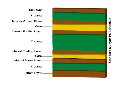
Optimizing PCB Layout for Energy Efficiency: Design Techniques for a Greener Future
PCB layout energy efficiency techniques help electrical engineers reduce power consumption and improve thermal management in PCB design. Explore low power PCB layout and green PCB design practices for sustainable, reliable electronics that lower energy use and extend device life.
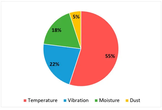
Improving the Reliability of Navigation System PCBs in Harsh Environments
Conformal coating, environmental testing, thermal management, vibration resistance, and humidity control strengthen navigation PCB reliability in harsh environments. Electric engineers gain practical strategies to prevent failures from temperature swings, shocks, and moisture for durable navigation systems.
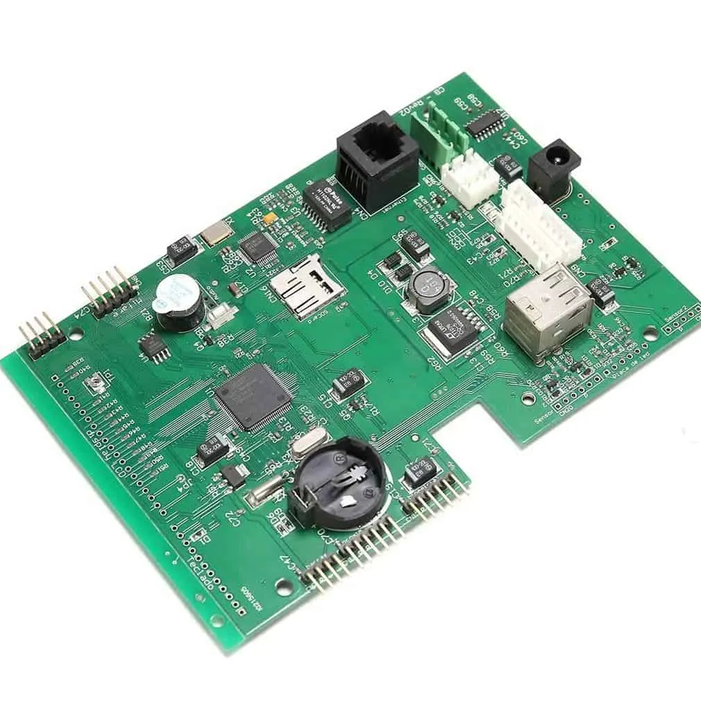
Step by Step Guide to Prototyping Your Navigation System PCB
Master navigation PCB prototyping services with this step by step guide for electronic hobbyists. Learn schematic design, quick turn PCB fabrication, assembly, and testing to build reliable GPS trackers, drone controllers, or robot navigators in days.
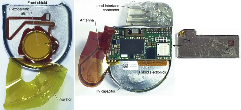
Optimizing Power Management in Pacemaker PCBs: Efficient Battery Usage for Long Term Reliability
Low power PCB design for pacemakers reduces consumption and extends battery life in medical implants. Strategies include power management ICs, optimized layouts, energy harvesting, and best practices for reliable pacemaker PCB performance over a decade.

The Role of Design for Manufacturing (DFM) in Reducing Waste and Energy Consumption
Design for Manufacturing (DFM) cuts waste and energy consumption in PCB production through panelization, symmetric stackups, and optimized routing. Factory insights and standards guide electrical engineers toward DFM PCB sustainability, reduce waste PCB manufacturing, and efficient PCB production practices.
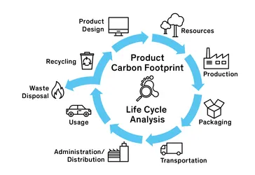
From Cradle to Grave: Analyzing the Environmental Impact of PCB Materials
Examine the environmental impact of FR-4 PCB materials from raw extraction through manufacturing, use, and disposal challenges. Compare alternative PCB substrates, biodegradable PCB materials, and eco-friendly PCB laminates. Practical guidance on material selection PCB supports engineers in creating sustainable designs while meeting performance needs.
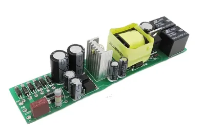
The Ultimate Guide to Railway Signaling PCB Design Standards (EN 50129)
This guide covers EN 50129 PCB compliance for railway signaling, detailing Safety Integrity Levels, design principles, best practices, certification processes, and CENELEC standards to help electric engineers create reliable PCBs for harsh railway conditions.
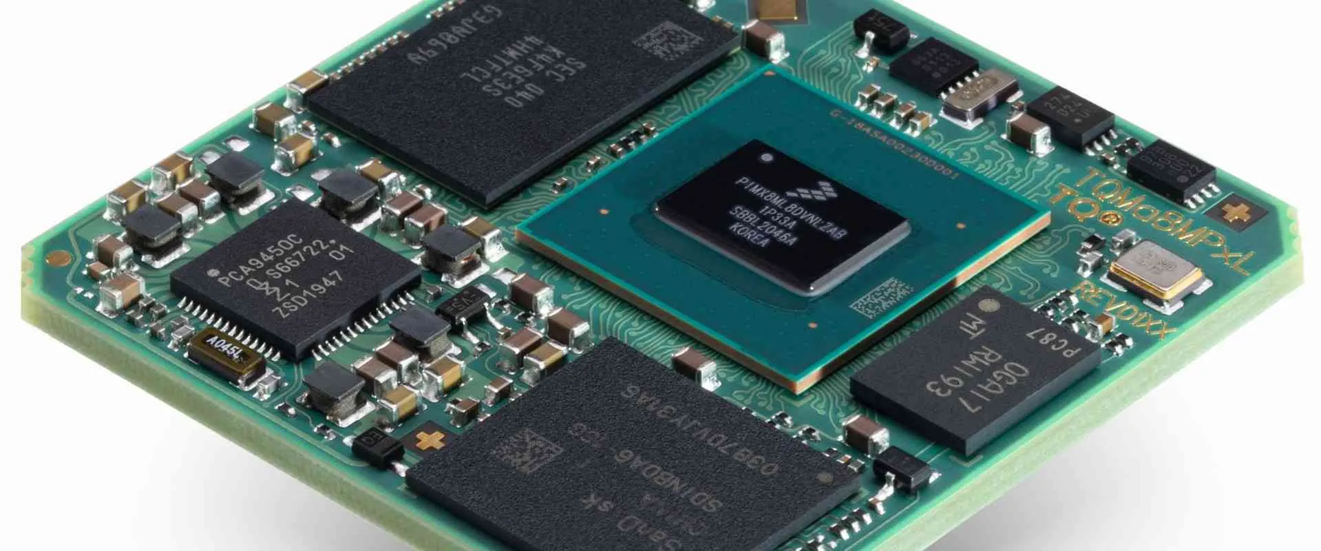
Railway Signaling PCB Troubleshooting: Common Issues and Solutions
Railway signaling PCBs deal with signal loss, component failure, and thermal management faults from vibration and EMI. Find PCB fault finding techniques using oscilloscopes, thermal imaging, and inspections plus repair solutions for troubleshooting railway electronics and system reliability.
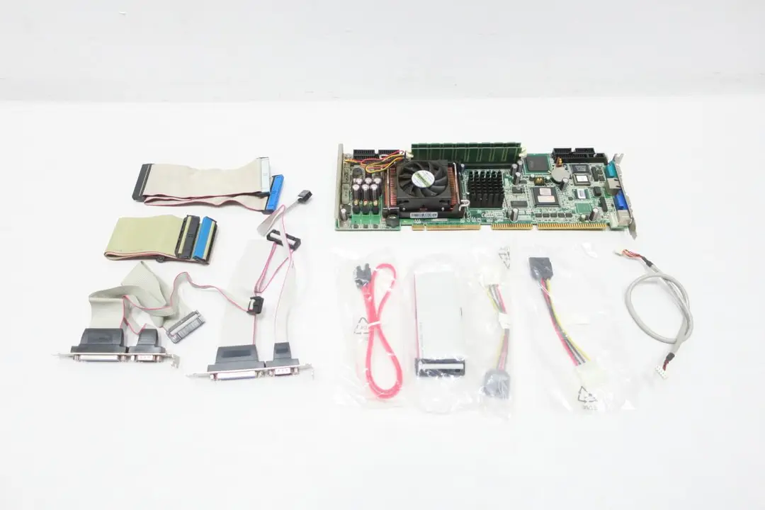
Wind Turbine Control PCB Cost Optimization: Strategies for Efficient Manufacturing
Engineers apply PCB cost reduction strategies to lower wind turbine PCB manufacturing costs without sacrificing reliability. Learn design tips, material choices, supply chain practices, and standards for optimizing PCB production in harsh environments. Achieve efficient manufacturing for control systems.
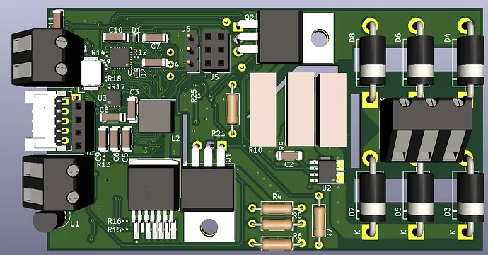
Advanced SMT Assembly Techniques for Wind Turbine Control PCBs
High-reliability SMT assembly for wind turbine control PCBs handles vibration, humidity, and corrosion. Techniques cover BGA assembly with X-ray checks, conformal coating for protection, wave soldering for mixed boards, plus best practices and troubleshooting tips for engineers building robust systems.
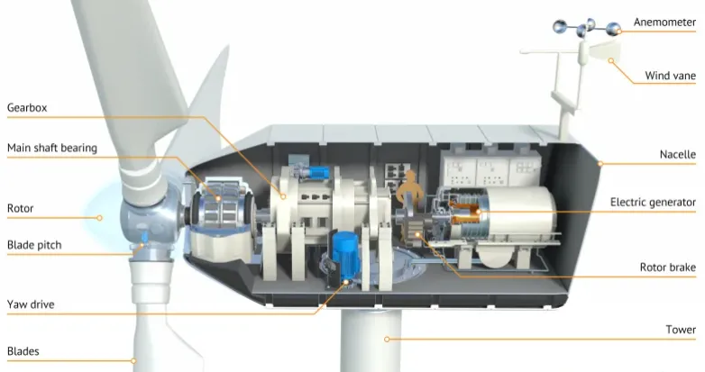
The Ultimate Guide to Wind Turbine Control PCB Design for Harsh Environments
Wind turbine PCB design guidelines for harsh environments focus on PCB environmental protection, conformal coating for wind turbines, and PCB corrosion resistance. Build reliable control boards that handle salt spray, vibration, humidity, and temperature swings for maximum uptime.
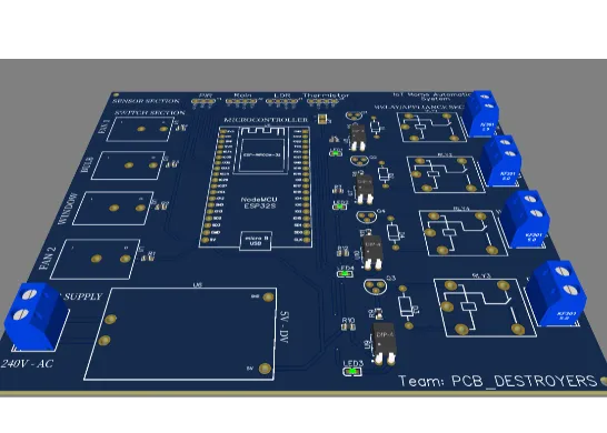
Signal Integrity Challenges in High Speed Smart Home Device PCBs
High-speed smart home PCBs face signal integrity issues from crosstalk, EMI, and impedance mismatches. Get practical high speed PCB layout tips, impedance matching techniques, and EMI reduction strategies to achieve reliable gigabit data transmission in compact devices for electric engineers.


