


PCB Manufacturing
Printed Circuit Boards (PCBs) form the backbone of modern electronics, serving as the essential platform where components connect to create functional devices. In the PCB Manufacturing category, readers gain access to a comprehensive collection of resources designed to demystify the intricate processes involved in producing these critical elements. From initial design considerations to final assembly and testing, this category covers every stage, providing valuable insights for engineers, hobbyists, and industry professionals alike. Understanding PCB manufacturing is crucial for anyone involved in electronics development. This field encompasses a wide range of topics, including material selection, such as FR-4 substrates and advanced laminates, as well as fabrication techniques like etching, drilling, and soldering. Articles here delve into best practices for optimizing layouts to minimize signal interference, ensuring reliability in high-stakes applications. Tutorials guide users through prototyping methods, while in-depth analyses explore emerging trends like flexible PCBs and additive manufacturing, which are revolutionizing industries from consumer gadgets to aerospace systems. The practical value of mastering PCB manufacturing extends to real-world scenarios, where efficient production can reduce costs, enhance performance, and accelerate time-to-market. For instance, insights on multilayer board construction help in designing compact devices for IoT applications, and discussions on quality control standards prevent common pitfalls in mass production. By engaging with the diverse guides and expert perspectives in this category, readers can build a solid foundation in PCB technologies, apply proven strategies to their projects, and stay ahead in an ever-evolving field. Whether troubleshooting assembly issues or exploring sustainable manufacturing practices, the knowledge shared here empowers informed decision-making and innovation in electronics.
Latest Blogs
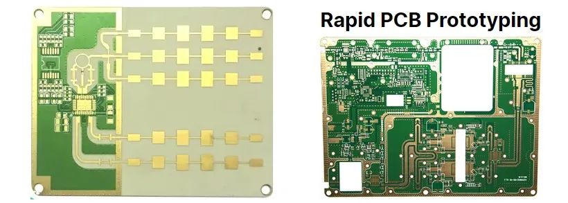
Unlock Rapid Innovation: The Power of On Demand PCB Manufacturing for Prototyping
On-demand PCB prototyping services deliver fast turn PCB prototypes and assembly for electrical engineers. Covers PCB design for rapid prototyping, fabrication steps, best practices, challenges, standards like IPC-6012E, and FAQs for efficient workflows.
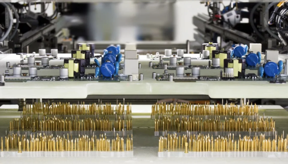
Understanding the Bed of Nails In Circuit Testing
Learn how bed of nails PCB tests ensure high-quality, reliable circuit boards. Explore testing principles, fixture design, practical factory implementation, and best practices to maximize coverage and minimize defects.

PCB Reflow Soldering and Component Orientation: Minimizing Defects
Master component orientation in PCB reflow soldering to minimize tombstoning, shadow effect, and thermal mass defects. Learn practical placement guidelines, conveyor direction rules, spacing recommendations, and profiling best practices per IPC/J-STD standards for higher SMT yields.
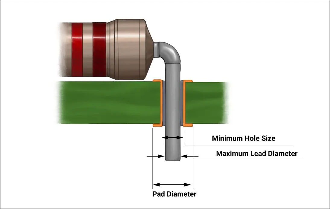
Achieving Consistent Hole Fill in PCB Wave Soldering: Tips and Techniques
Achieve reliable PCB wave soldering hole fill with practical tips on capillary action, solder wicking prevention, and plated through hole optimization. Cover preheat profiles, flux selection, conveyor settings, and troubleshooting for complete barrel fill and robust PTH joints in assembly processes.
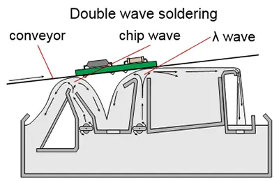
Understanding the Double Wave in PCB Wave Soldering: Benefits and Applications
The PCB wave soldering double wave pairs turbulent chip wave for lead cleaning and hole fill with laminar wave for smooth joints. It counters shadow effects in dense through-hole boards for higher yields. Electric engineers gain practical insights on benefits, applications in power supplies and controls, plus troubleshooting aligned with IPC standards.

PCB Wave Soldering for Hobbyists: A Beginner's Guide to Through-Hole Assembly
PCB wave soldering DIY tutorial for hobbyists explains through-hole assembly at home. Covers setup with solder pot and flux, step-by-step process, safety tips, best practices, common defects like bridges, and fixes for strong joints every time.
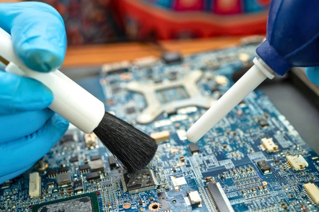
PCB Cleaning for High-Frequency Applications: Minimizing Signal Loss and Maximizing Performance
PCB cleaning for high-frequency circuits reduces signal loss due to contamination on traces and dielectrics. Key methods include ultrasonic and vapor cleaning for RF boards, with steps for impedance control in PCB cleaning and testing PCB performance after cleaning using ROSE, SIR, TDR, and VNA for reliable results.

The Environmental Impact of PCB Automation: Sustainable Manufacturing Practices
Cut environmental impact in PCB production with eco-friendly PCB automation. Learn how automation reduces waste in manufacturing, minimizes energy use, and applies sustainable assembly practices. Key technologies and best practices for electric engineers to implement green processes effectively.

Ensuring Quality Control in Automated PCB Assembly
Proven quality control in automated PCB assembly covers automated PCB testing methods like AOI and AXI, quality assurance techniques, defect prevention strategies, statistical process control for PCB, and real-time monitoring. Essential for engineers seeking reliable high-yield production.
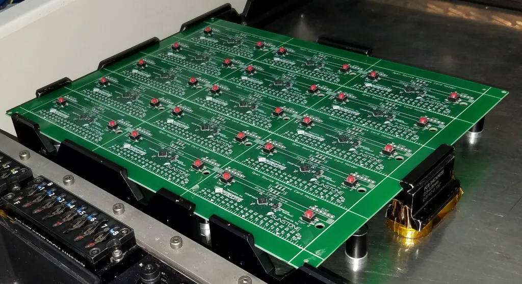
Optimizing PCB Design for Automated Manufacturing
DFM for PCB automation, PCB design rules for automated assembly, best PCB layout practices for automation, Gerber file optimization for automation, and CAD/CAM for PCB automation enable efficient high-volume production. Electric engineers gain practical guidance to minimize defects, boost yields, and streamline assembly lines.
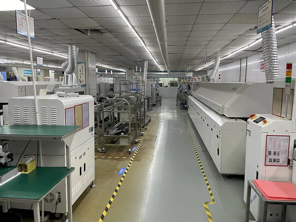
Cost Effective Halogen Free PCB Manufacturing: Strategies and Solutions
Practical guide to reducing halogen-free PCB cost through smart material selection, design optimization, and process controls. Compare halogen vs non-halogen PCB costs and implement solutions for affordable halogen-free PCBs in production. Ideal for engineers seeking reliable results.
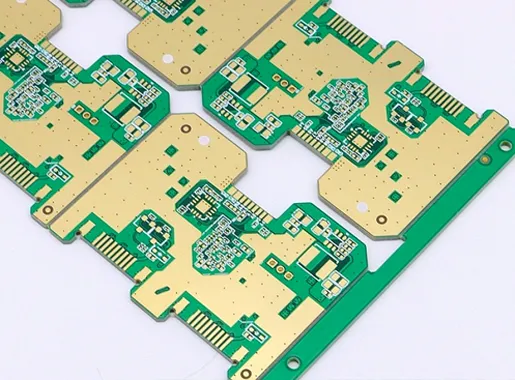
The Impact of Halogen Free PCBs on Signal Integrity: What Engineers Need to Know
Halogen-free PCB signal integrity depends on dielectric constant, dissipation factor, signal loss, and impedance matching in high-frequency PCB design. Electric engineers get practical best practices, stackup tips, standards like IPC-4101, and troubleshooting for reliable performance. (187 characters)


