HDI PCB Materials
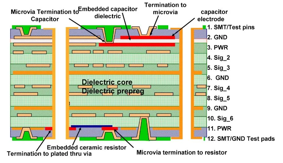
High Density Interconnect (HDI) PCBs represent a cornerstone of modern electronics design, enabling compact, high-performance circuitry in devices ranging from smartphones to automotive systems. At the heart of these advanced boards are HDI PCB materials, which include specialized substrates, laminates, prepregs, and copper foils engineered for fine-line features, microvias, and multilayer constructions. These materials must withstand rigorous demands such as thermal stability, signal integrity, and mechanical durability, making them essential for applications where space constraints and reliability are paramount. For engineers and designers searching for insights on HDI PCB materials, this tag serves as a comprehensive resource, delving into the properties that influence board performance and manufacturability. Selecting the right HDI PCB materials involves evaluating factors like dielectric constant, coefficient of thermal expansion (CTE), and glass transition temperature (Tg) to ensure compatibility with high-speed signals and harsh environments. For instance, halogen-free laminates offer environmental benefits while maintaining low loss for RF applications, whereas resin-coated copper (RCC) foils facilitate buried and blind vias in dense layouts. Practical applications highlight their value: in consumer electronics, these materials support miniaturization without sacrificing functionality, while in aerospace, they provide robustness against vibration and temperature extremes. Best practices recommend starting with material data sheets from trusted suppliers like Rogers or Isola, followed by simulation tools to predict performance before prototyping. By exploring the articles linked under this tag, readers can gain actionable guidance on material selection, common pitfalls in HDI fabrication, and emerging trends such as advanced composites for 5G and IoT devices. Whether youre optimizing a new design or troubleshooting an existing one, these resources offer the technical depth needed to make informed decisions and achieve superior results in high-density PCB projects.
Technical Articles
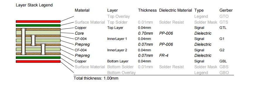
Advanced PCB Materials: Enhancing Blind and Buried Via Performance
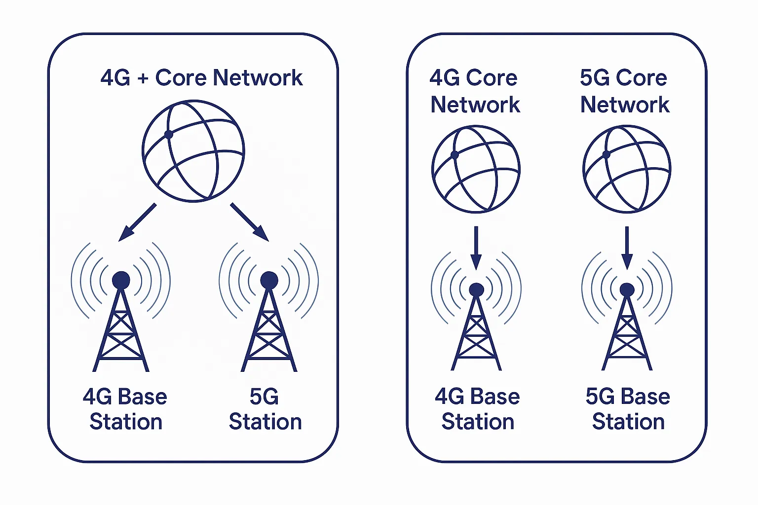
Advanced 5G Technologies: Network Slicing, RedCap, VoNR, and PCB Design Requirements for High-Performance Implementation
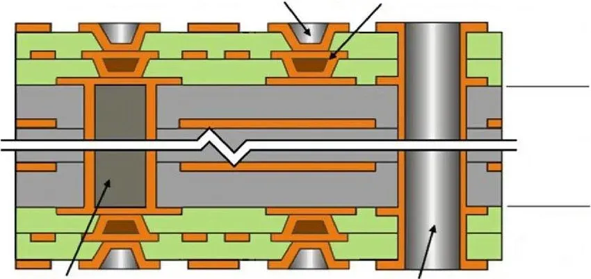
Advanced HDI PCB: Materials, Manufacturing, Design, and Interconnect Technology
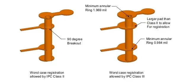
HDI PCB Standards: IPC Class 2 vs Class 3 for HDI Manufacturing
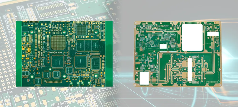
Standard HDI vs Automotive HDI: Manufacturing Differences
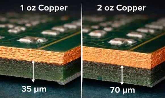
1oz vs 2oz Copper Thickness for HDI PCB: Which One Should You Choose?
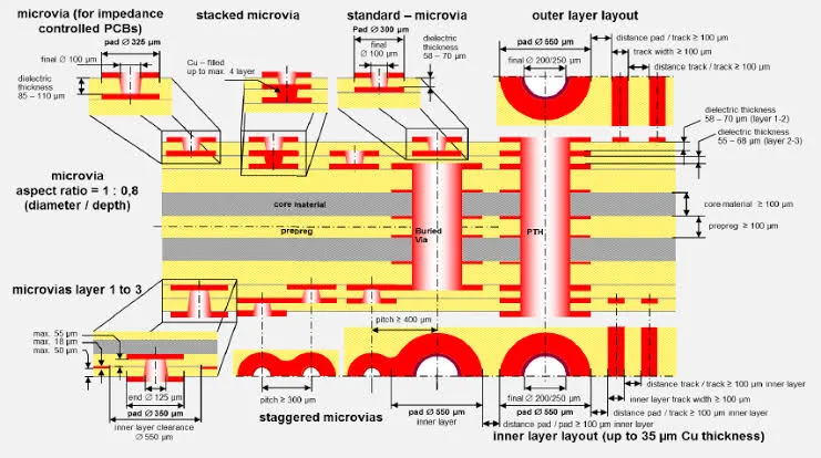
Shengyi vs Kingboard Materials for HDI PCB Manufacturing
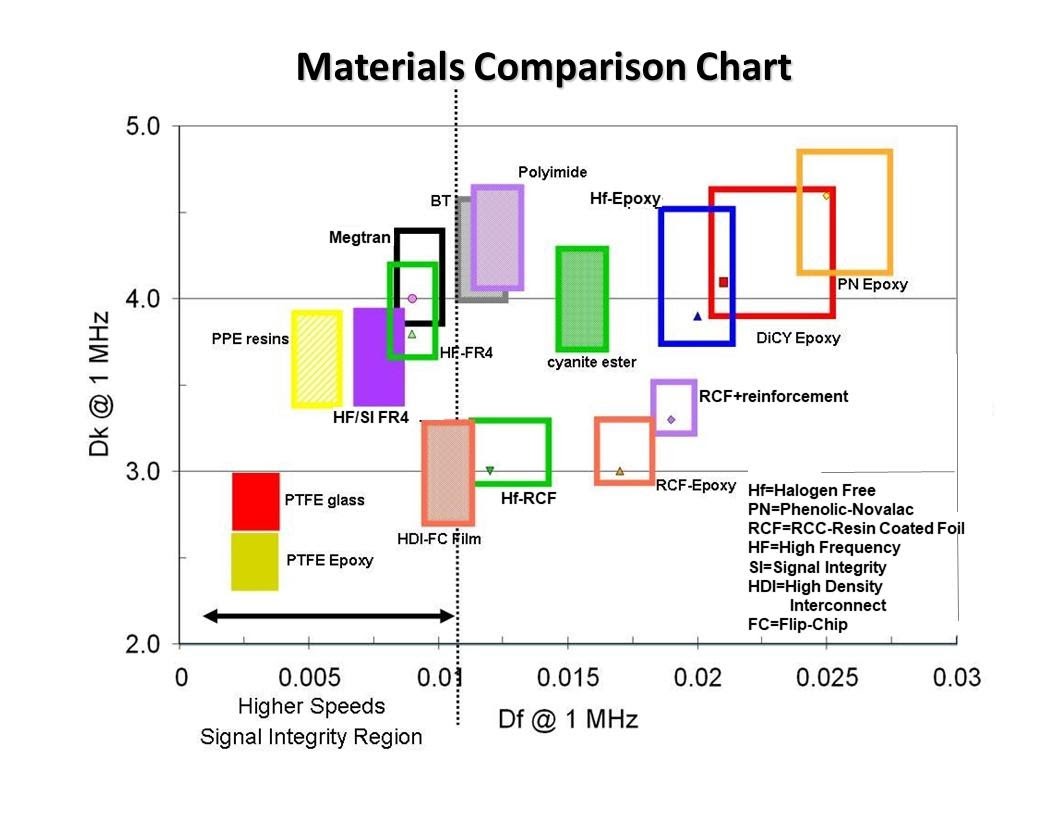
HDI Stackup Material Selection Mistakes That Increase Cost and Lead Time
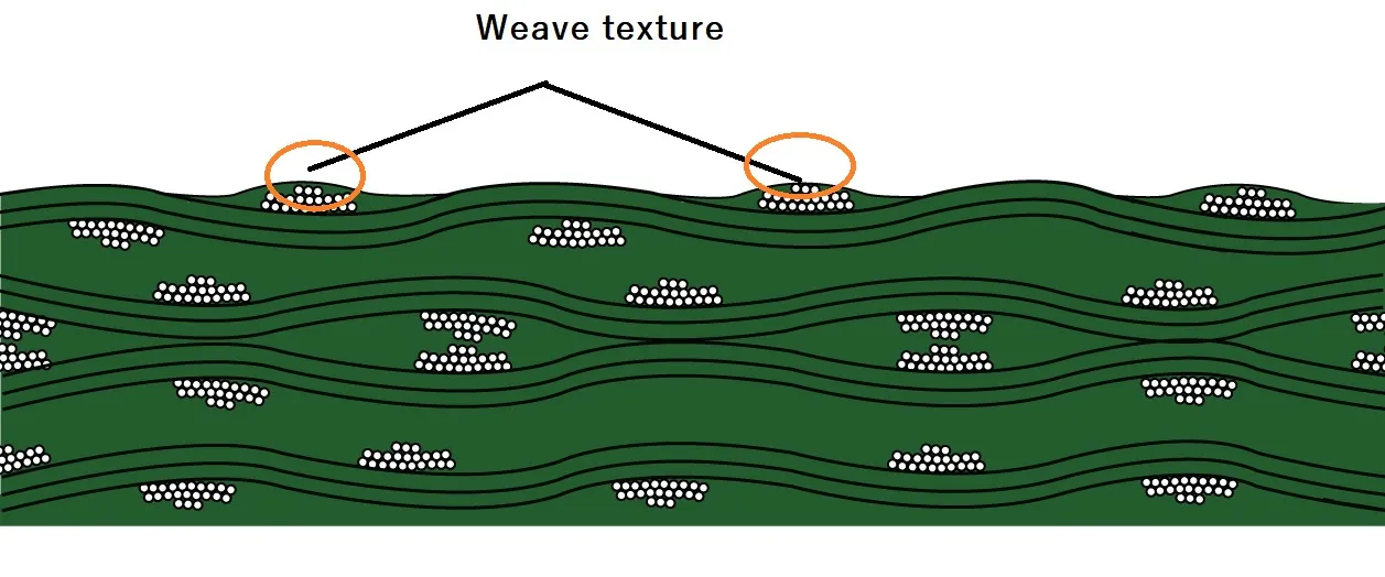
Beyond FR 4: Selecting the Right Materials for High Performance HDI PCBs
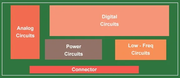
HDI Multilayer PCB Design: Advanced Techniques for High-Density Boards
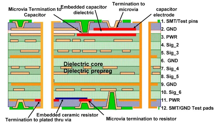
HDI PCB Materials Selection for High Frequency Applications
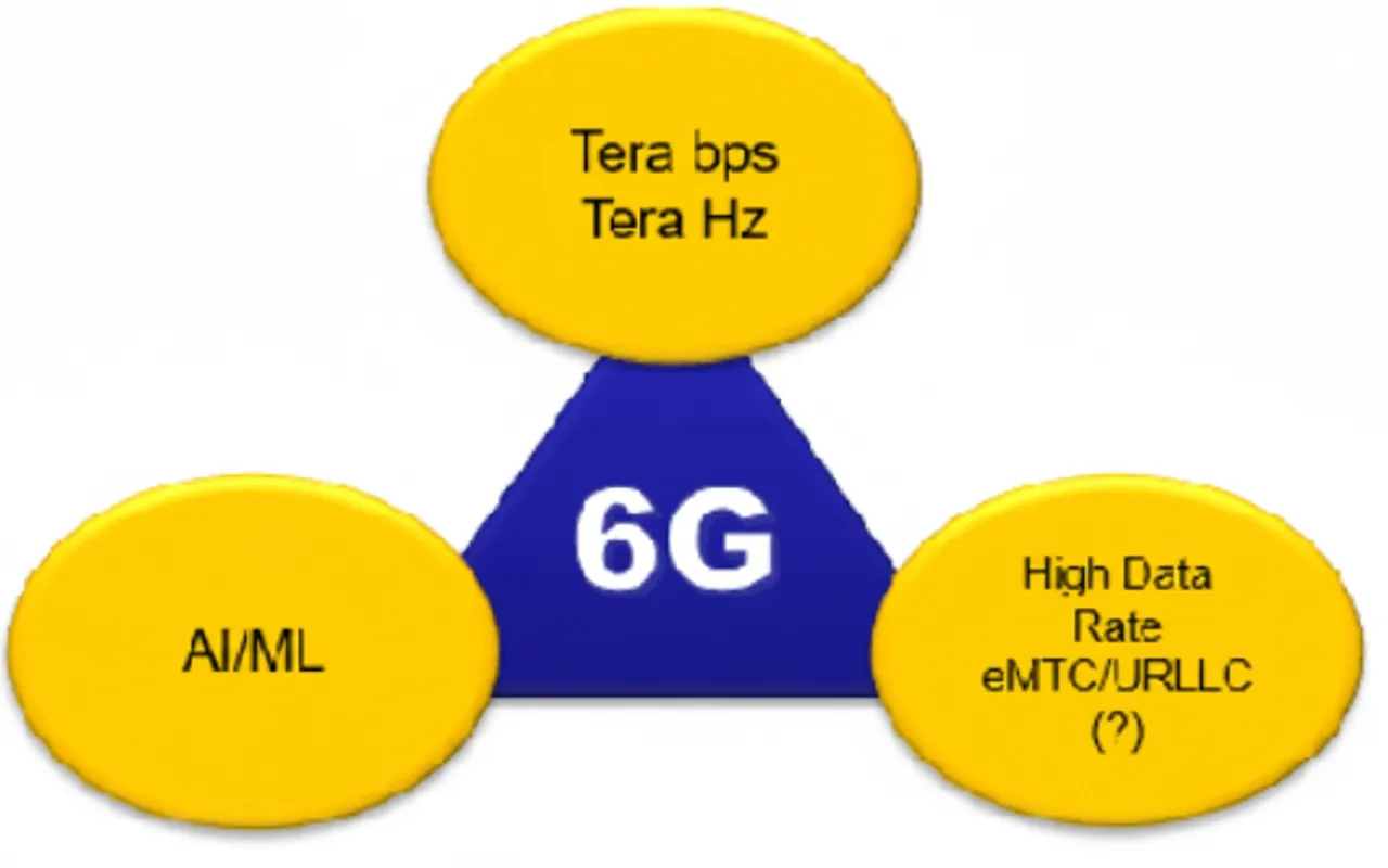
6G Mobile Communications: PCB Design, 3D Integration, and Manufacturing Challenges for THz, AI-Native, and Massive MIMO Systems
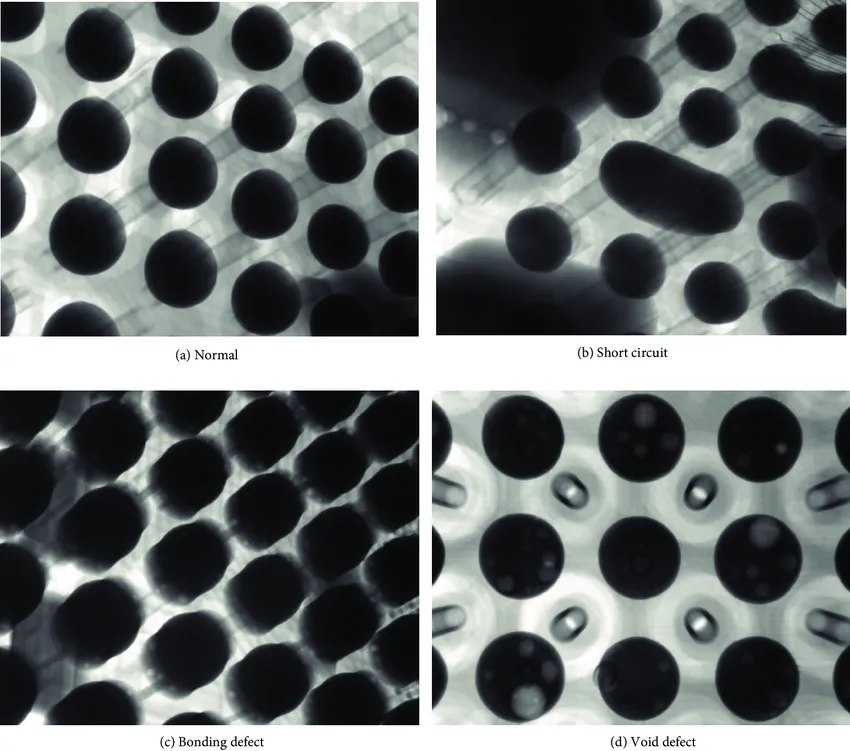
HDI PCB X-Ray Inspection for Assemblies: SMT Defect Detection and Quality Control
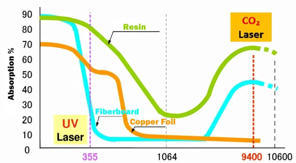
HDI PCB Laser Drilling: Materials, Techniques, and Equipment
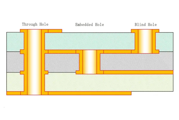
Advanced PCB Materials for Blind and Buried Vias: Enhancing Reliability and Performance
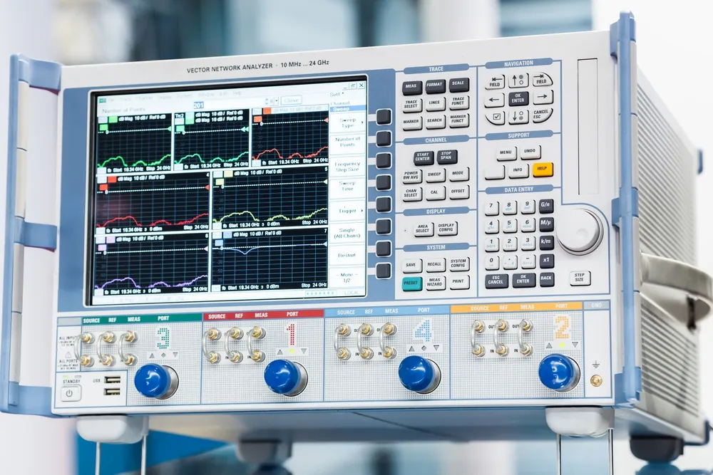
HDI Assembly: Selecting the right materials
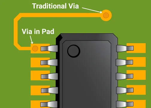
Troubleshooting Common Via-in-Pad Issues in PCB Design
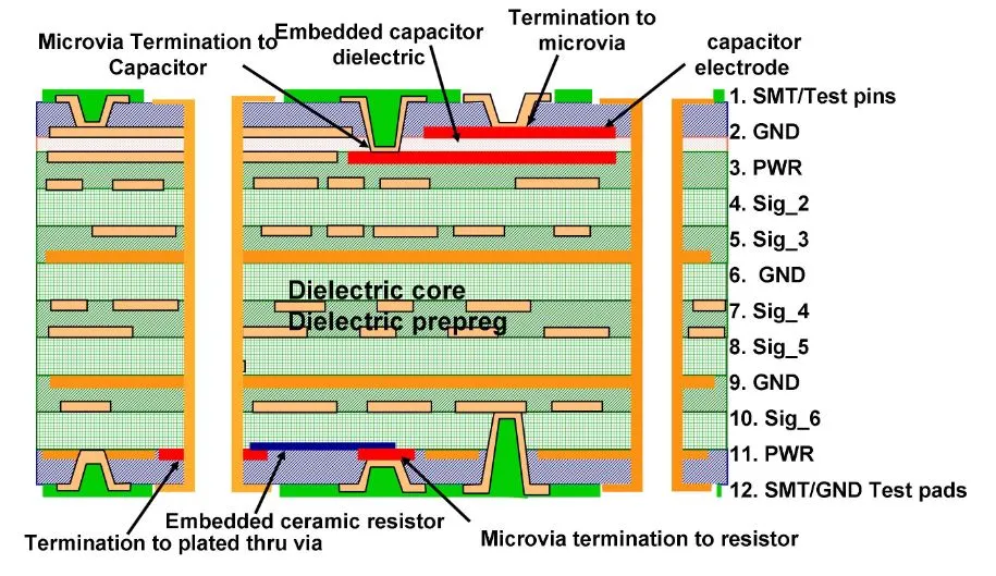
HDI Assembly: Stack Up Structures and Materials