


PCB Assembly
Printed circuit board (PCB) assembly represents a critical phase in electronics manufacturing, where components are mounted onto a board to create functional circuits. This process bridges design and production, ensuring that electronic devices perform reliably in diverse applications. From soldering techniques to component placement, PCB assembly encompasses the methods and technologies that transform bare boards into operational systems. Understanding these elements is essential for engineers, hobbyists, and industry professionals aiming to optimize production efficiency and product quality. Within this category, readers will find a comprehensive collection of guides that detail step-by-step assembly processes, tutorials on advanced tools like surface-mount technology and automated pick-and-place machines, and insights into troubleshooting common issues such as solder joint defects or thermal management challenges. Best practices are highlighted to promote reliability, including strategies for minimizing defects through quality control measures and adhering to industry standards like IPC guidelines. These resources draw from real-world expertise to address both fundamental concepts and cutting-edge innovations in the field. The practical value of mastering PCB assembly extends to numerous sectors, including consumer electronics, automotive systems, medical devices, and aerospace engineering. By applying the knowledge shared here, professionals can reduce manufacturing costs, accelerate time-to-market, and enhance device durability. For instance, effective assembly techniques ensure that circuits withstand environmental stresses, leading to longer-lasting products in demanding conditions. Delving into the articles in this PCB assembly category provides a pathway to deeper technical proficiency. Whether refining prototyping skills or scaling up production, the content equips readers with actionable strategies to tackle real-world challenges and stay ahead in an evolving industry.
Latest Blogs
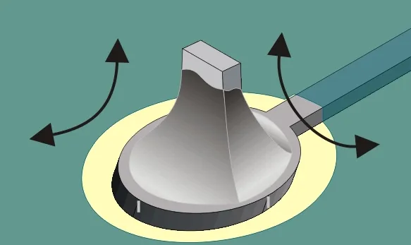
Fundamentals of Solder Joint Metallurgy in SMT: Concepts, Formation, and Performance
SMT solder joint metallurgy: formation (wetting, diffusion), performance metrics, and how alloy, base metals, and process parameters affect reliability.
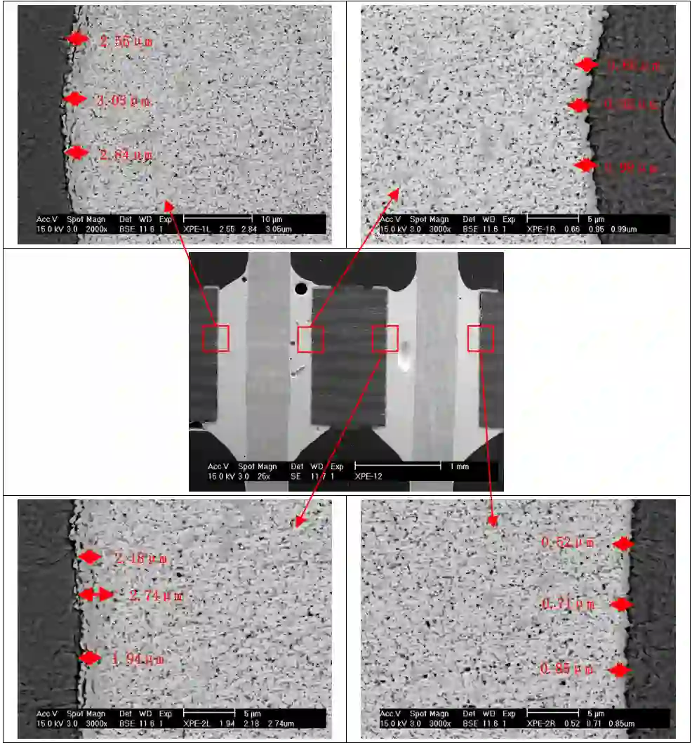
SMT Failure Analysis of a Power PCB: Metallographic Cross-Section and Copper Thickness Report
Metallographic and SEM failure analysis of a power PCBA finds nonconforming solder joints, PTH copper, and trace thickness against IPC-6012D/IPC-A-610J Class 2.

SMT Process Design for QFN Exposed-Pad Vias and Reflow Soldering Validation
QFN thermal via design and stencil guidance with reflow validation to reduce voiding and prevent package shift; covers land sizing and solder mask options.

Key Process Controls for Wave Soldering in PCBA
Wave soldering process control in PCBA: flux spray, pot temperature, wave geometry, conveyor speed, temperature profiling, and maintenance to stabilize quality and yield.
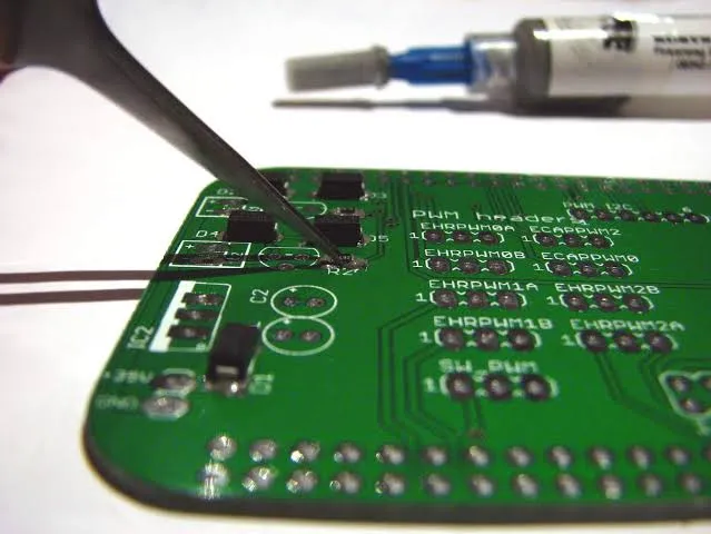
Understanding SMT Soldering Fundamentals: Surface Wetting and Solderability
Explains wetting and solderability in PCB assembly: contact angle, flux and atmosphere effects, intermetallic formation, testing methods, and reflow profile controls.
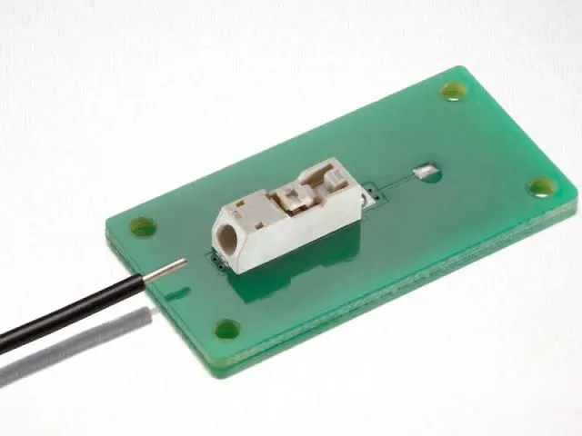
SMT Electronic Connectors: Structures, Materials, and Characteristics for Process Engineers
SMT connectors: construction, housing materials, contacts, keying, and plating, with process guidance on reflow, solderability, and mechanical reliability in PCB assembly.
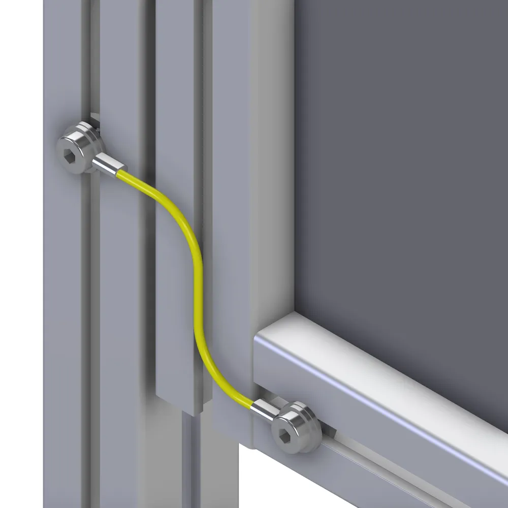
ESD Isolated Conductors: Definition and Measurement for SMT Engineers
Defines ESD isolated conductors per ANSI/ESD S20.20 and details surface voltage measurement (non-contact/contact), procedures, tools, risks, and mitigations in SMT.
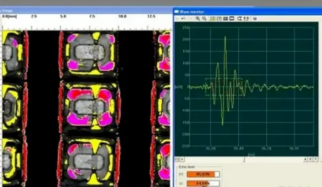
What Is C-SAM and How Does It Support SMT Process Analysis?
Explains C-SAM principles, SMT applications, and advantages in layer-specific defect detection, with a MOSFET failure analysis case and outlook on future improvements.
SMT PCB Dimensional Expansion and Shrinkage: Root Causes and Mitigation Strategies for Process Engineers
Technical guide to HDI PCB expansion and shrinkage: causes across cutting, imaging, lamination, laser, via plugging, solder mask, plus measured data and process controls.
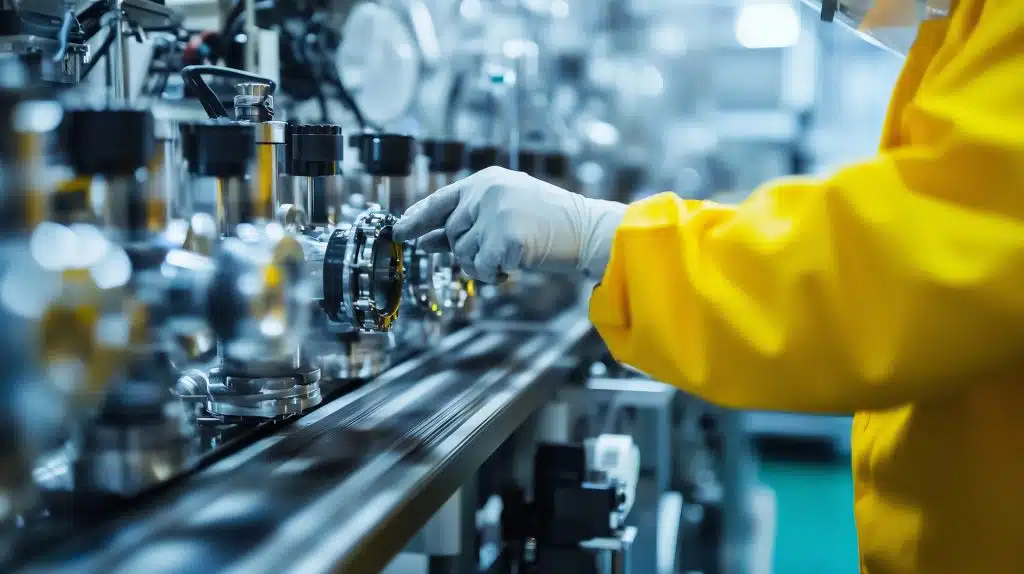
Lead Free Assembly in Industrial Applications: Optimizing for Harsh Environments
Master lead-free industrial PCB assembly for harsh conditions like vibration, heat, and corrosion. Get practical tips on components, soldering processes, and testing to build reliable industrial electronics that meet standards and last longer. Essential guide for engineers.
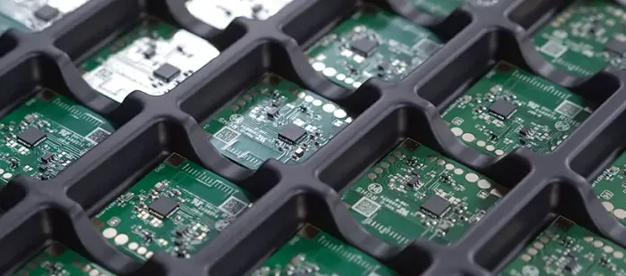
High Volume PCB Assembly: Ensuring Regulatory Compliance and Certifications
High volume PCB assembly demands PCB regulatory compliance with UL certification, CE marking, RoHS compliance and REACH compliance. Electric engineers find practical best practices, troubleshooting tips and standards to ensure safety, avoid recalls and meet global market requirements efficiently.
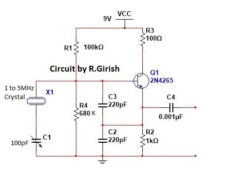
DIY Crystal Oscillators: Building Your Own Timing Circuits
Build your own DIY crystal oscillator with this step by step tutorial. Covers essential components, breadboard prototype, PCB layout tips, troubleshooting, and best practices for stable timing in hobbyist projects.


