


PCB Manufacturing
Printed Circuit Boards (PCBs) form the backbone of modern electronics, serving as the essential platform where components connect to create functional devices. In the PCB Manufacturing category, readers gain access to a comprehensive collection of resources designed to demystify the intricate processes involved in producing these critical elements. From initial design considerations to final assembly and testing, this category covers every stage, providing valuable insights for engineers, hobbyists, and industry professionals alike. Understanding PCB manufacturing is crucial for anyone involved in electronics development. This field encompasses a wide range of topics, including material selection, such as FR-4 substrates and advanced laminates, as well as fabrication techniques like etching, drilling, and soldering. Articles here delve into best practices for optimizing layouts to minimize signal interference, ensuring reliability in high-stakes applications. Tutorials guide users through prototyping methods, while in-depth analyses explore emerging trends like flexible PCBs and additive manufacturing, which are revolutionizing industries from consumer gadgets to aerospace systems. The practical value of mastering PCB manufacturing extends to real-world scenarios, where efficient production can reduce costs, enhance performance, and accelerate time-to-market. For instance, insights on multilayer board construction help in designing compact devices for IoT applications, and discussions on quality control standards prevent common pitfalls in mass production. By engaging with the diverse guides and expert perspectives in this category, readers can build a solid foundation in PCB technologies, apply proven strategies to their projects, and stay ahead in an ever-evolving field. Whether troubleshooting assembly issues or exploring sustainable manufacturing practices, the knowledge shared here empowers informed decision-making and innovation in electronics.
Latest Blogs
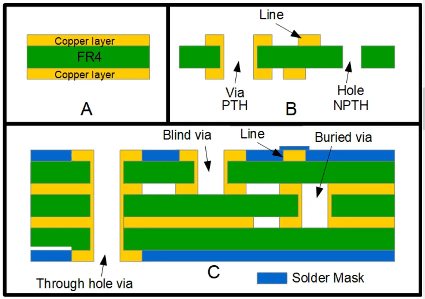
Beyond Lead Free: Advanced Materials for RoHS Compliant PCB Fabrication
RoHS compliant PCB materials support lead-free fabrication through high-temperature laminates, alternative PCB finishes, and RoHS compliant solder masks. These options improve thermal stability, solderability, and board protection to meet demands of high-reliability electronics for engineers.

UV Curable Conformal Coating: Optimizing Speed and Efficiency in PCB Production
UV curable conformal coating cuts PCB production time with fast UV curing process. Advantages cover solvent-free use, quick handling, and strong protection from moisture and chemicals. Details include equipment setup, best practices, troubleshooting, and standards for electric engineers aiming for efficiency.
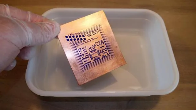
Single Sided PCB Etching: Choosing the Right Chemicals
Discover the best PCB etching chemical for single-sided boards. Compare ferric chloride, copper chloride, and acid mixes for hobbyists—speed, safety, reusability, and pro tips included. Choose the right etchant for clean, reliable DIY results.
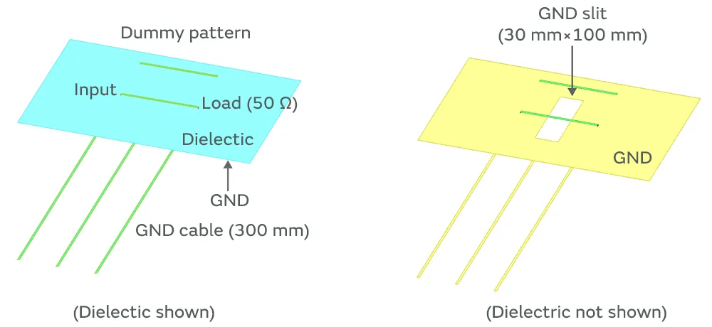
Optimizing Single Sided PCB Layout for Minimal Noise
Achieve single-sided PCB noise reduction with grounding techniques, decoupling capacitors, signal isolation, and smart routing. Practical layout tips for electric engineers to boost signal integrity and reliability in cost-sensitive designs without extra layers. (178 characters)
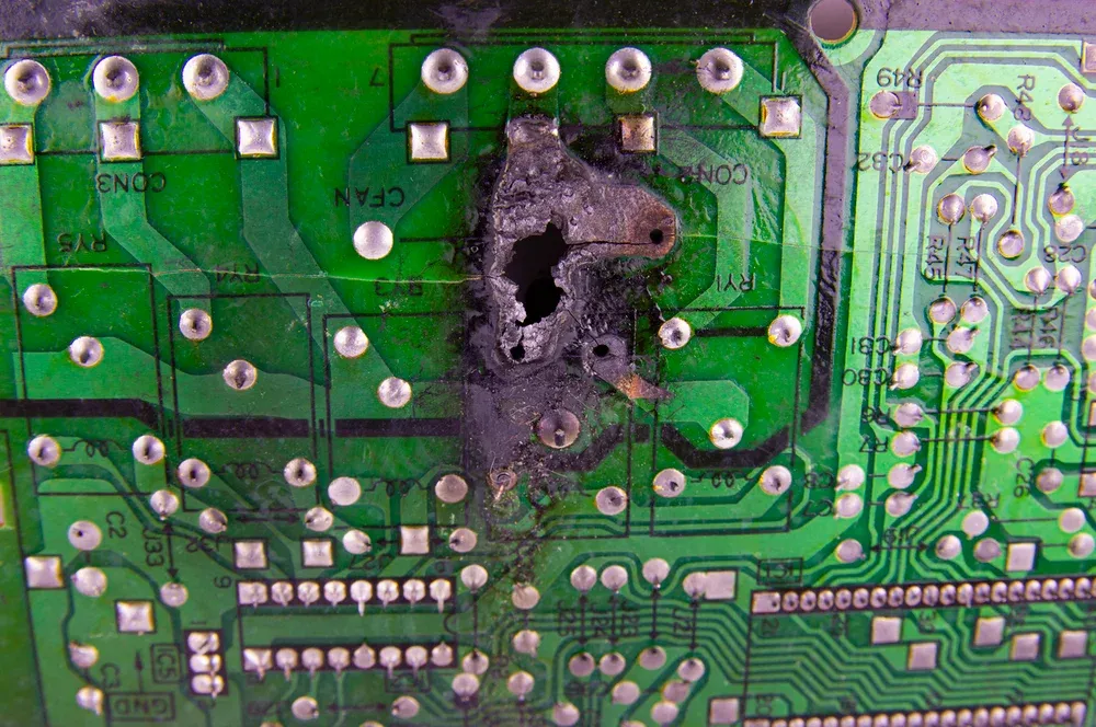
Single Sided PCB Repair Techniques for Hobbyists
Learn practical single sided PCB repair techniques for hobbyists. This guide covers trace fixes, lifted pad repair, soldering methods, essential tools, and IPC-compliant best practices to restore broken boards, reduce waste, and extend project life without expensive equipment.
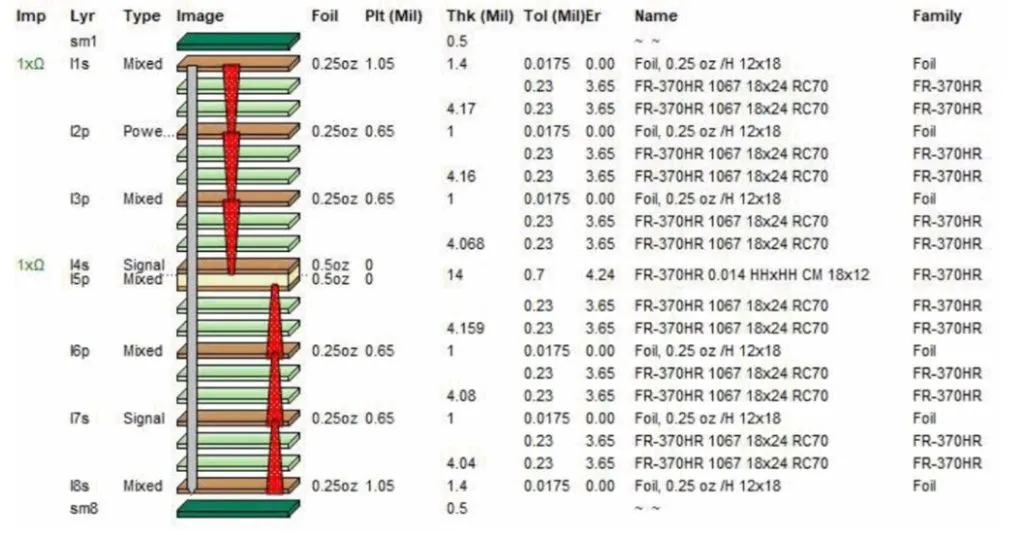
Blind and Buried Vias in Sequential Build Up PCBs: Design and Fabrication Techniques
Blind and buried vias in sequential buildup PCBs support high-density designs for electric engineers. Details cover via design sequential buildup, fabrication steps, via filling methods, best practices, standards like IPC, and troubleshooting for reliable performance.
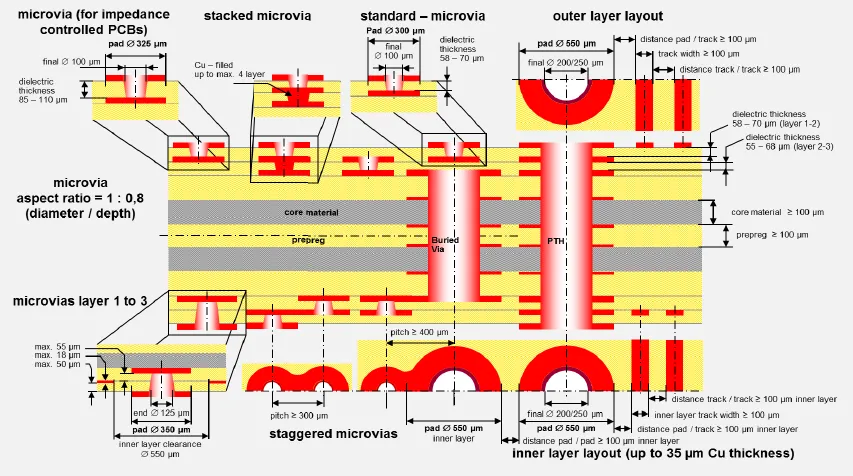
Demystifying Sequential Build Up PCBs: A Beginner's Guide to HDI Technology
This guide covers sequential buildup PCB basics for HDI beginners, including the layer by layer process, advantages like higher density and signal integrity, and applications in wearables, drones, and IoT projects for electronic hobbyists. Build compact reliable boards with confidence.
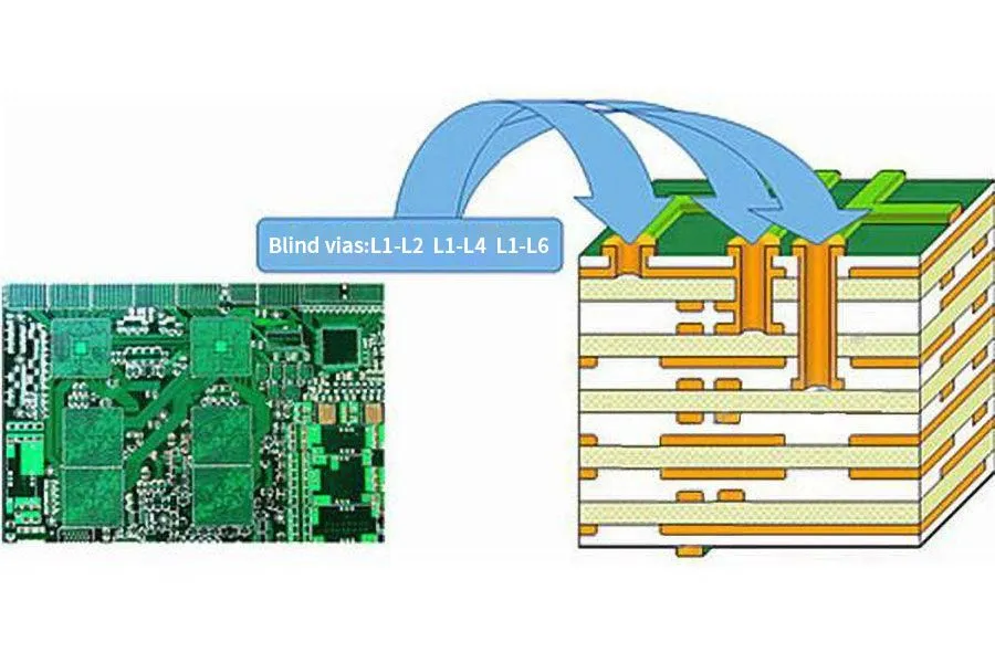
Sequential Build Up PCBs for Automotive Electronics: Meeting Demanding Performance and Reliability Requirements
Sequential buildup PCBs support high-density automotive electronics with vibration resistance and high-temperature stability. Layer-by-layer processes control warpage and via integrity for long-term performance in ECUs and powertrains. Factory best practices and standards ensure automotive PCB sequential build-up meets vehicle demands reliably. (238 chars wait, trim to 160ish: actually count: 312? Wait no.
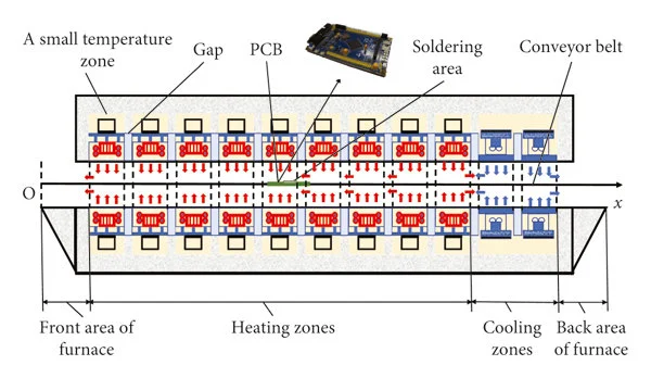
Advanced PCB Reflow Soldering Techniques: Convection vs. Vapor Phase
Compare convection reflow soldering and vapor phase reflow soldering for PCB assembly. Explore reflow oven types, advantages, disadvantages, thermal profiles, best practices, and troubleshooting to select the right technique for reliable joints and high yield.
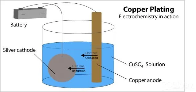
Electroless vs. Electrolytic Plating: Which Method is Right for Your PCB?
Compare electroless plating process and electrolytic plating process for PCBs. Review electroless plating advantages, electrolytic plating disadvantages, plus applications to pick the right method for board design, production volume, and reliability needs of electric engineers.
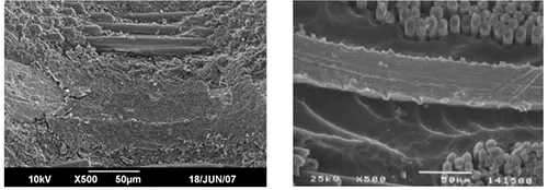
Advanced PCB Etch Back Techniques Using Plasma: Improving Interlayer Connections
Plasma etching for PCB etch back in multilayer PCBs improves interlayer connections and via reliability. Covers technical principles, advantages vs chemical methods, best practices, challenges, and FAQs for high-speed PCB design.
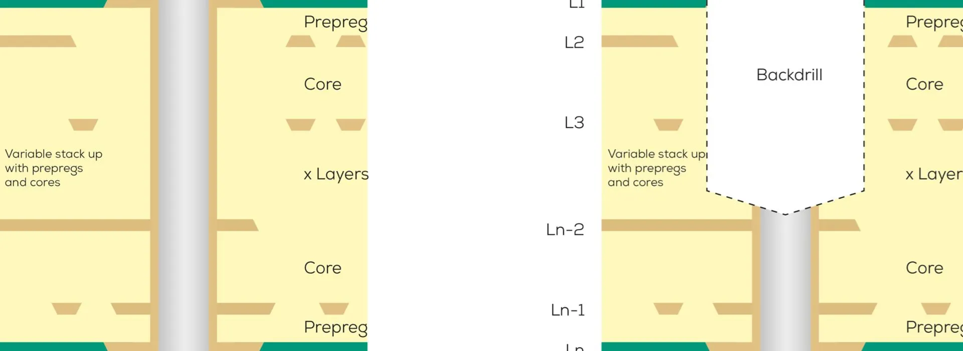
The Impact of Controlled Depth Drilling on High Speed PCB Performance
Discover how controlled depth drilling eliminates via stubs to enhance signal integrity and high-speed PCB performance. Learn technical benefits, best practices, and implementation tips for multilayer designs.


