


PCB Manufacturing
Printed Circuit Boards (PCBs) form the backbone of modern electronics, serving as the essential platform where components connect to create functional devices. In the PCB Manufacturing category, readers gain access to a comprehensive collection of resources designed to demystify the intricate processes involved in producing these critical elements. From initial design considerations to final assembly and testing, this category covers every stage, providing valuable insights for engineers, hobbyists, and industry professionals alike. Understanding PCB manufacturing is crucial for anyone involved in electronics development. This field encompasses a wide range of topics, including material selection, such as FR-4 substrates and advanced laminates, as well as fabrication techniques like etching, drilling, and soldering. Articles here delve into best practices for optimizing layouts to minimize signal interference, ensuring reliability in high-stakes applications. Tutorials guide users through prototyping methods, while in-depth analyses explore emerging trends like flexible PCBs and additive manufacturing, which are revolutionizing industries from consumer gadgets to aerospace systems. The practical value of mastering PCB manufacturing extends to real-world scenarios, where efficient production can reduce costs, enhance performance, and accelerate time-to-market. For instance, insights on multilayer board construction help in designing compact devices for IoT applications, and discussions on quality control standards prevent common pitfalls in mass production. By engaging with the diverse guides and expert perspectives in this category, readers can build a solid foundation in PCB technologies, apply proven strategies to their projects, and stay ahead in an ever-evolving field. Whether troubleshooting assembly issues or exploring sustainable manufacturing practices, the knowledge shared here empowers informed decision-making and innovation in electronics.
Latest Blogs
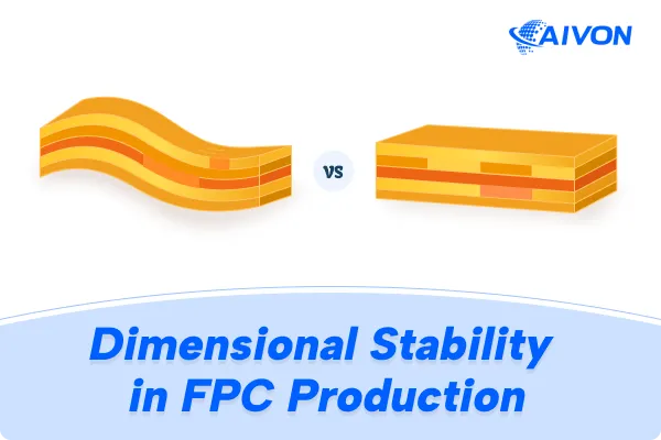
Dimensional Stability in FPC Manufacturing: Causes and Solutions
Learn what dimensional stability means in FPC manufacturing and how materials, moisture, temperature, copper distribution, lamination, and artwork compensation affect dimensional accuracy.
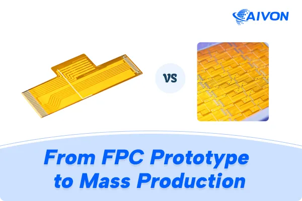
From FPC Prototype to Mass Production: Manufacturing Considerations
Moving an FPC from prototype to mass production requires more than increasing order volume. earn how flexible PCB prototyping supports design validation, manufacturing review, and mass production.Explore key FPC prototype considerations with AIVON.
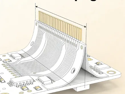
Why HDI PCB Warpage Increases With Uneven Layer Structures
How asymmetric stackups, copper imbalance and CTE mismatch drive HDI PCB warpage in production. CAM copper balancing, lamination stress relief and process limits factories actually use.
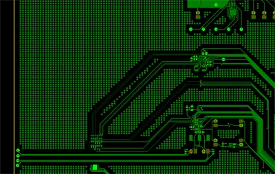
HDI PCB Copper Balance: Why Uneven Copper Distribution Matters
From the CAM and plating floor, how HDI copper balance is enforced to stop warpage, thickness variation, and yield loss when copper density is uneven across the panel.
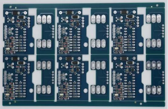
How to Prevent Solder Bridging on Fine-Pitch HDI BGA Pads
From the fab floor: how CAM sets SMD pads, mask web limits and registration to stop HDI BGA solder bridging on 0.4 mm pitch and tighter before the boards ever reach SMT.
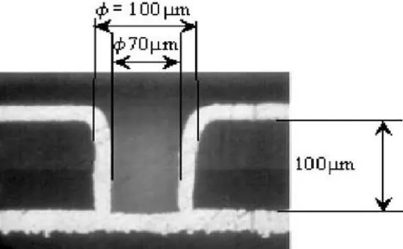
How Small Can an HDI Microvia Be Before Manufacturing Becomes Risky?
The practical minimum microvia diameter HDI is set by plating reliability and aspect ratio, not laser limits. Stay above 75 µm with design margins to avoid voids, thin copper and reliability failures.

HDI BGA Pad Clearance Problems That Can Delay Production
Factory view on HDI BGA pad clearance: how CAM catches tight clearances, why registration stack-up creates short risks, and the process controls that stop yield loss and shipment delays.
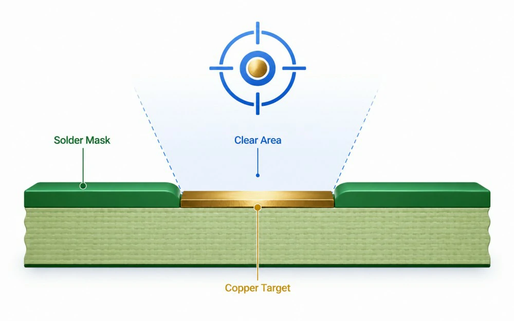
Why HDI PCB Fiducial Placement Matters for Assembly Accuracy
HDI fiducial placement decides SMT accuracy on high-density boards. See the exact CAM rules, local mark positions near BGAs, and what fails when marks are missing or covered.
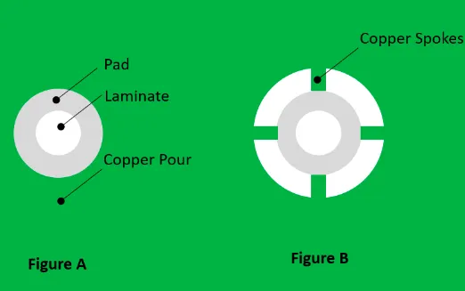
HDI Thermal Relief Design: When Should You Use It?
From PCB production: when HDI thermal relief is applied on via/pad-to-plane connections for controlled soldering heat, how CAM sets spoke widths, and when solid connections stay.
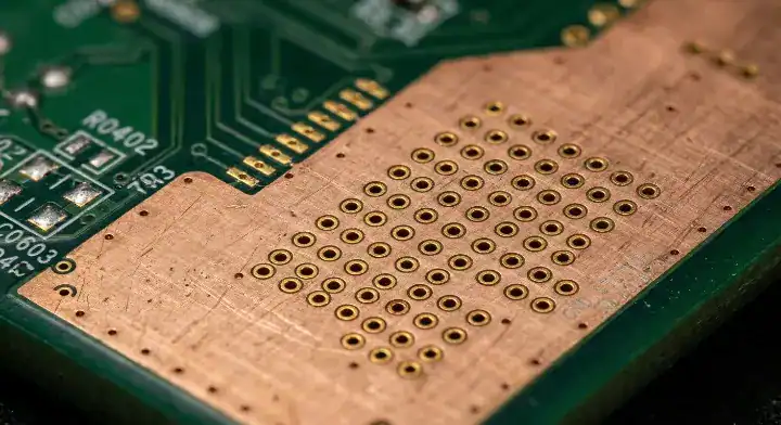
HDI Copper Pour Clearance: Common Layout Mistakes to Avoid
Factories enforce 3.5–5 mil HDI copper pour clearance after etch. See why tight pour-to-via/pad gaps cause shorts, how CAM compensates, and when exceptions are allowed.
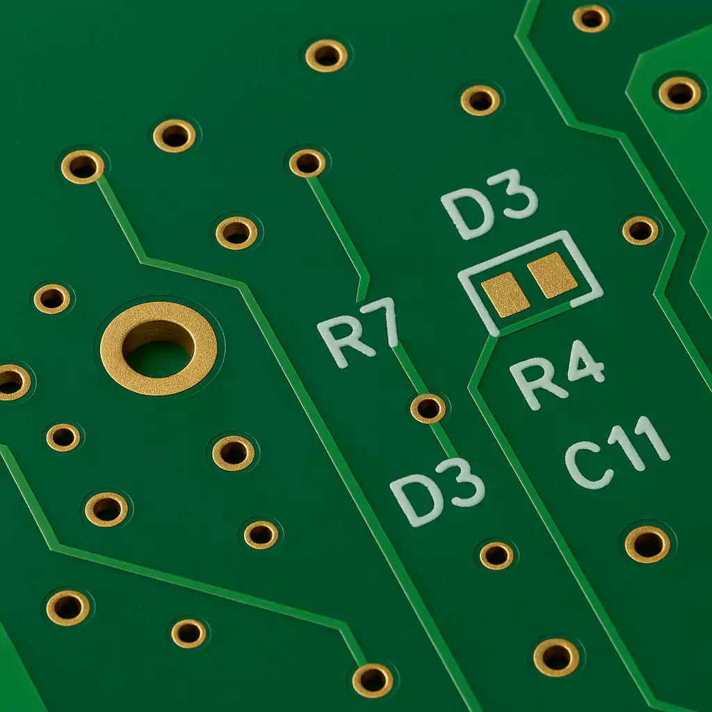
HDI Solder Mask Expansion: Common CAM Review Problems
Factory view on HDI solder mask expansion: why CAM flags oversize or undersize openings, pad bridging risk on fine pitch, and the exact expansion window (0.025–0.05 mm) we enforce to protect yield.
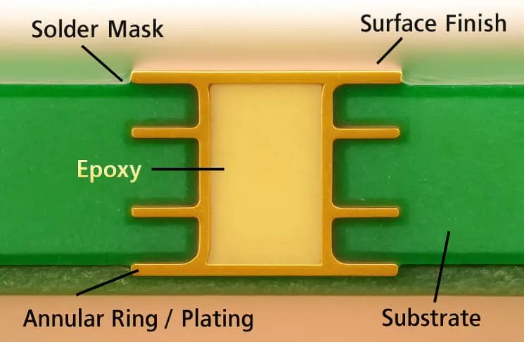
How to Avoid Solder Mask Issues Around HDI Microvias
Factory method for HDI microvia solder mask: CAM opening expansion, registration compensation, bridging control and residual-ink checks that protect soldering yield.


