 00:47
00:47
Enig Finish
ENIG finish, or Electroless Nickel Immersion Gold, is a widely adopted surface treatment for printed circuit boards (PCBs) that enhances solderability, corrosion resistance, and overall reliability in electronic assemblies. This tag page gathers articles and resources focused on ENIG finish, offering in-depth insights for engineers, designers, and manufacturers seeking to optimize PCB performance in demanding applications. By applying a thin layer of nickel followed by immersion gold, ENIG provides a flat, uniform surface that excels in high-density interconnects and fine-pitch components, making it ideal for industries such as telecommunications, automotive electronics, and consumer devices where long-term durability is essential. For those searching for information on ENIG finish, understanding its practical advantages can guide better decision-making in PCB fabrication. Unlike other finishes like HASL (Hot Air Solder Leveling), ENIG avoids issues such as uneven surfaces or thermal stress, ensuring consistent soldering results during assembly. Key benefits include excellent shelf life, resistance to oxidation, and compatibility with lead-free soldering processes, which are critical for meeting RoHS compliance standards. In practice, designers should consider factors like board thickness, via types, and environmental exposure when specifying ENIG; for instance, it performs exceptionally well in humid or corrosive environments but may require careful masking to prevent gold migration in certain designs. Professionals often turn to ENIG for its balance of cost and performance, particularly in prototypes and high-volume production runs. Best practices include selecting reputable fabricators with precise control over immersion processes to minimize defects like black pad syndrome, and conducting thorough testing for intermetallic compound formation. Through the articles linked here, you can delve into case studies, troubleshooting tips, and comparisons with alternatives like OSP or immersion tin, helping you apply these insights directly to your projects for improved outcomes.
Video Guide
-
00:47
Technical Articles
PCB Reliability Testing for SMT: Methods, Criteria, and Process Controls

ENIG "Black Pad" and BGA Solder Reliability: Failure Mechanism, Process Controls, and Acceptance Criteria
Basic PCB Concepts Needed to Start a Design
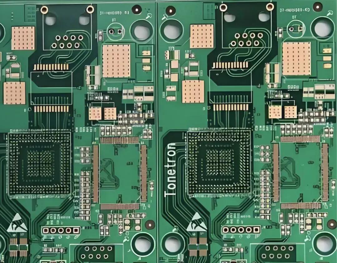
Why Are BGA Areas on a PCB Treated Differently?
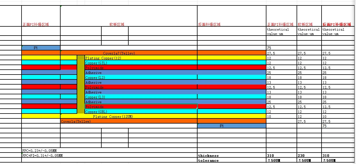
0.1 mm Finger Extension for Coverlay Retention on a 4-Layer Flexible Circuit
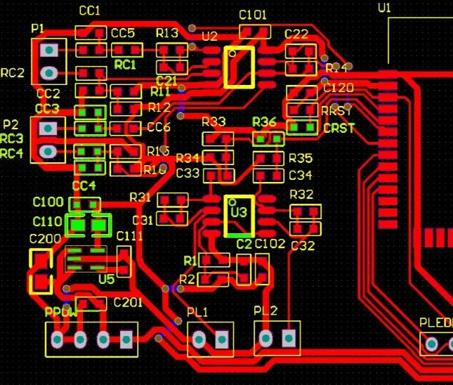
Should PCB Silkscreen Printing or ENIG Surface Finish Come First After Solder Mask?

When Bottom Silkscreen and PI Stiffener Specs Conflicted on a 0.2 mm 4-Layer Flexible PCB

Causes, Hazards, and Mitigation of Kirkendall Voids in Solder Joints

Key Manufacturing Technologies for Drone PCBs

8-Layer FR-4 PCB with Blind Vias: Solder Mask Openings, Via Plugging and V-CUT Clearance Issues During CAM Review
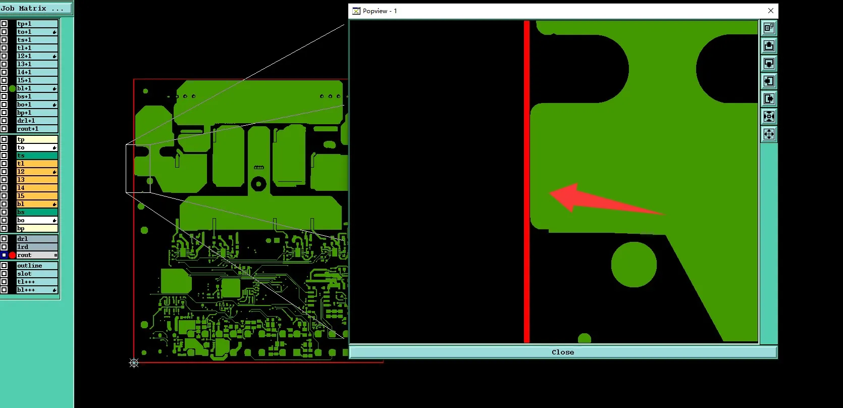
6-Layer 2oz Heavy Copper FR-4 PCB Engineering Review: Edge Clearance, Hole Attribute Conflicts and Silkscreen Overlap Case
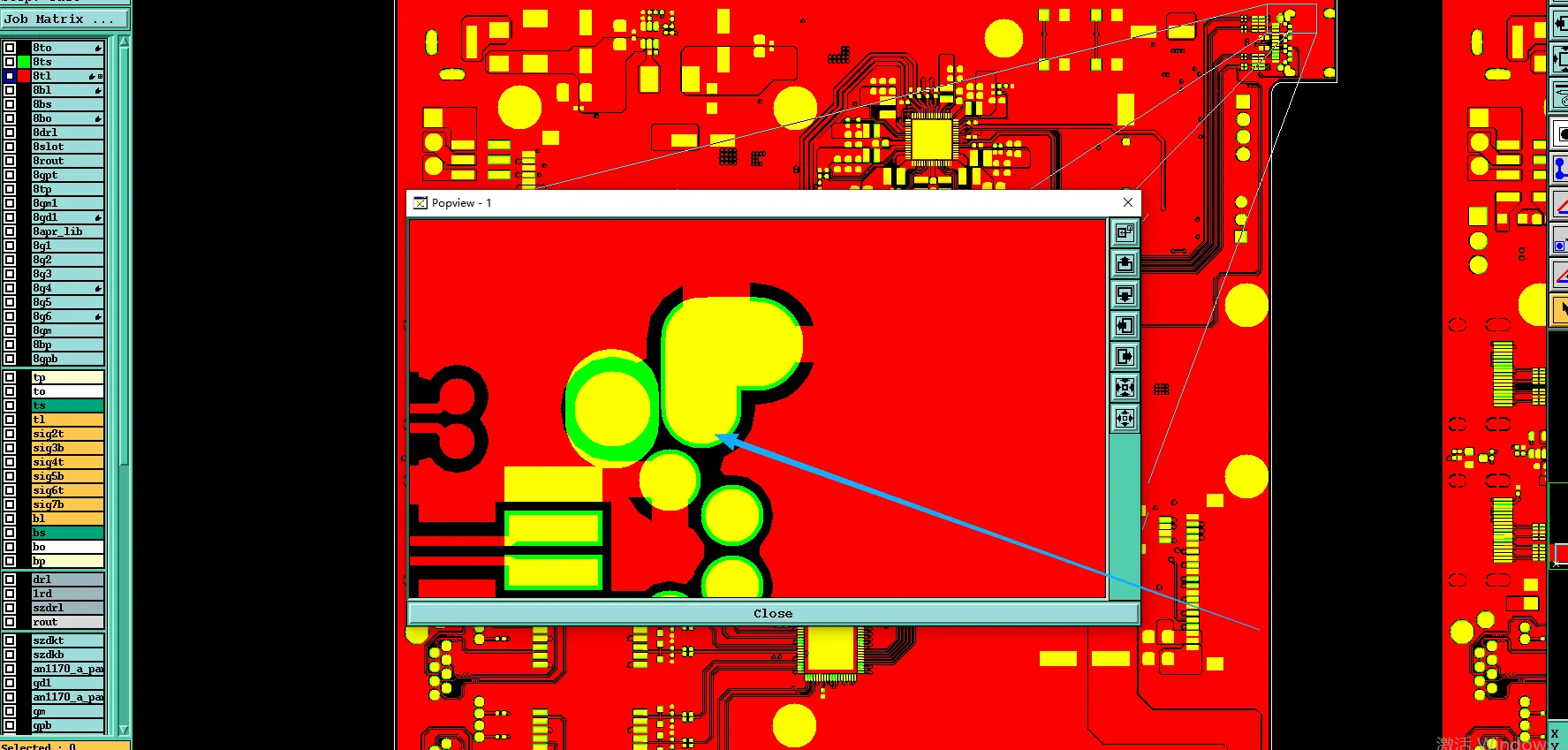
How to Fix Tight Pad Spacing and Impedance EQs in 8-Layer PCB CAM Review
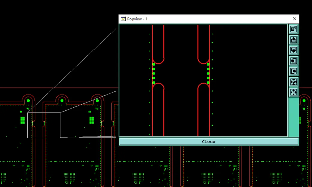
How to Prevent Solder Mask Bridge Failure and NSMD BGA Issues in 8-Layer PCB

4-Layer FR-4 TG170 PCB Case Study: Copper Overhang, Panelization & Legend Sizing Challenges During CAM Review
4-Layer High-TG PCB Stackup, Panelization & Mask Issues Fixed
How to Prevent Warpage in 4-Layer 2oz FR-4 TG170 PCB with Proper Stackup and V-CUT
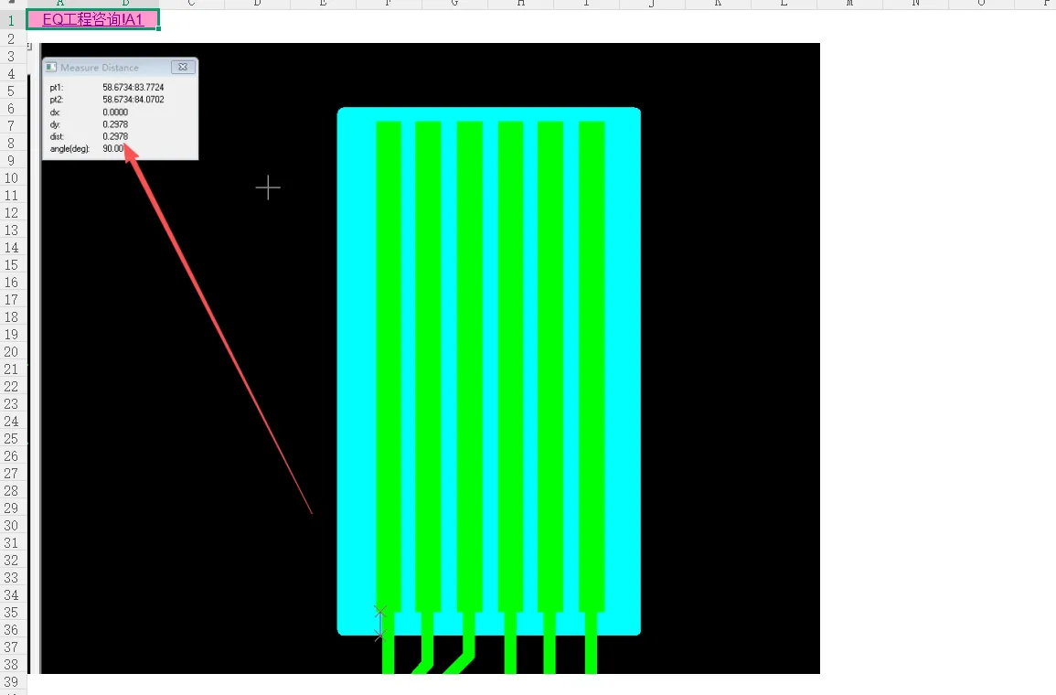
FPC Stiffener Design Rules: Avoiding Insertion Finger Failure
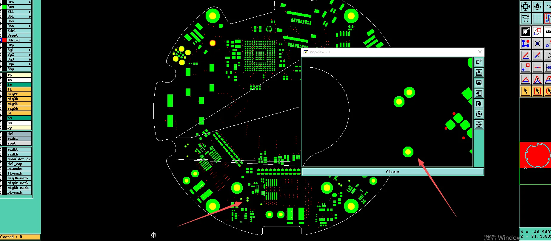
Avoiding DFM Delays: A Guide to PCB Resin Filled Via Design
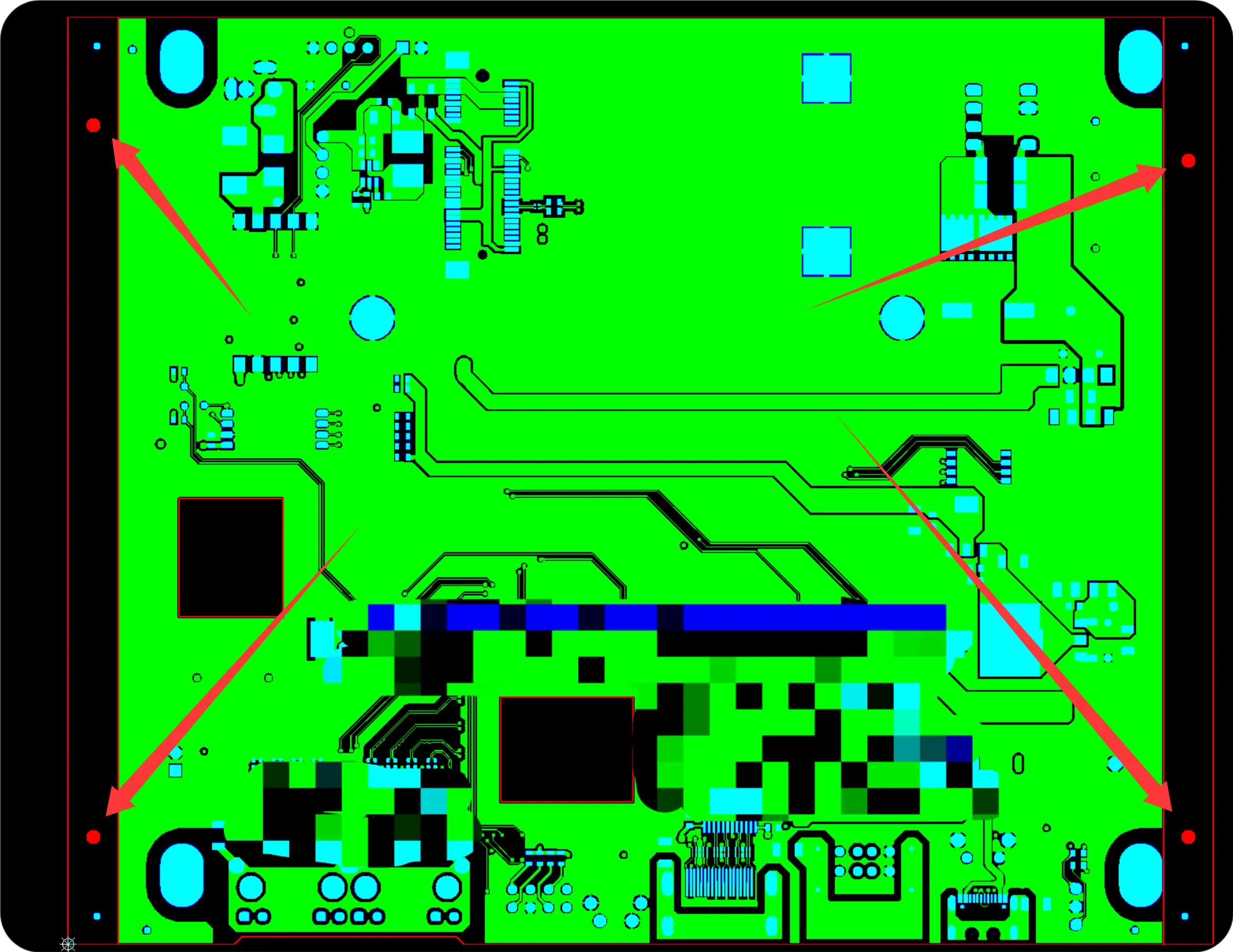
Handling PCB Impedance Trace Width Adjustment in DFM Review