 03:34
03:34
Multilayer PCB
Multilayer PCBs represent a cornerstone of modern electronics design, enabling the creation of compact, high-performance circuits that power everything from smartphones to industrial machinery. These boards consist of multiple layers of conductive copper separated by insulating materials, allowing for intricate routing of signals and power without the space constraints of single or double-layer alternatives. For engineers and designers searching for multilayer PCB solutions, this tag serves as a comprehensive resource, offering insights into their construction, advantages, and implementation strategies. One key benefit of multilayer PCBs is their ability to support higher component density, which is essential for devices requiring complex interconnections while minimizing electromagnetic interference. In practice, this means you can achieve better signal integrity and thermal management, crucial for applications in telecommunications, automotive systems, and medical equipment. When designing a multilayer PCB, focus on layer stackup planning to optimize impedance control and reduce crosstalk; for instance, alternating signal and ground planes can significantly enhance performance. Best practices also include using via structures like blind or buried vias to connect layers efficiently, avoiding common pitfalls such as uneven copper distribution that could lead to warping during fabrication. Professionals often turn to multilayer PCBs for their scalability in prototyping and mass production, where cost-effectiveness hinges on selecting appropriate materials like FR-4 or high-frequency laminates based on the project's demands. This tag compiles articles that delve into these topics, from step-by-step design tutorials to case studies on troubleshooting manufacturing issues. By reviewing the content here, you can gain practical knowledge to refine your projects, whether you're optimizing a new prototype or scaling up for commercial use.
Video Guide


Technical Articles

Single-Layer vs Multilayer PCB: Key Differences in Design and Applications

8-Layer PCB vs 6-Layer PCB: When Should You Choose Eight Layers?
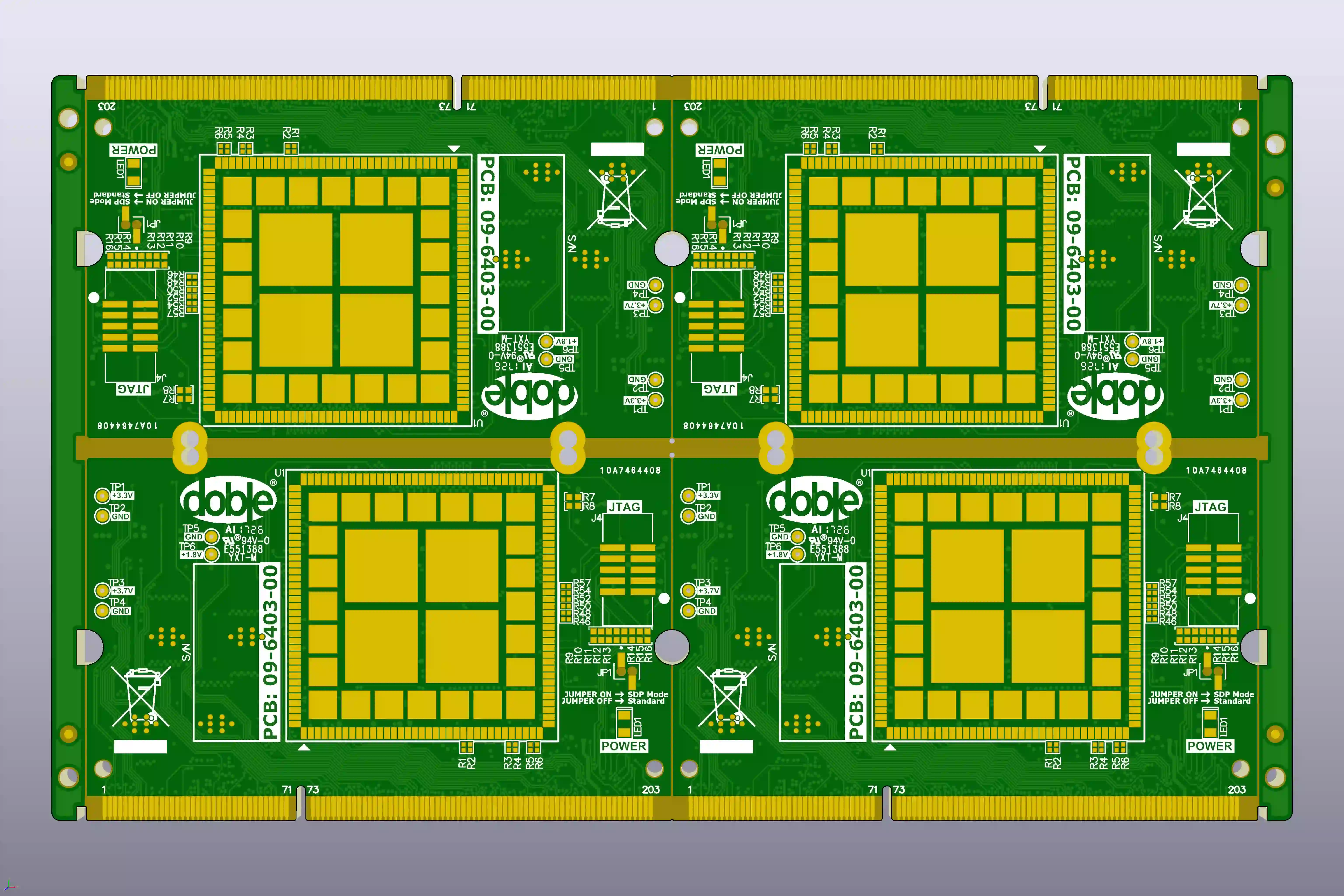
How to Resolve Gold Finger Bevel and Impedance EQs in 10-Layer PCBs

8-Layer FR-4 PCB with Blind Vias: Solder Mask Openings, Via Plugging and V-CUT Clearance Issues During CAM Review
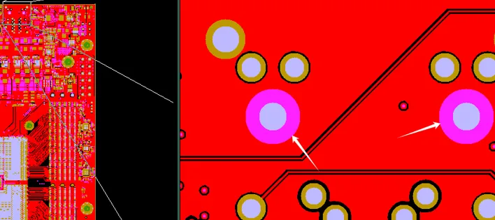
14 Layer TG170 PCB Manufacturing Review for Impedance and Resin Plugging
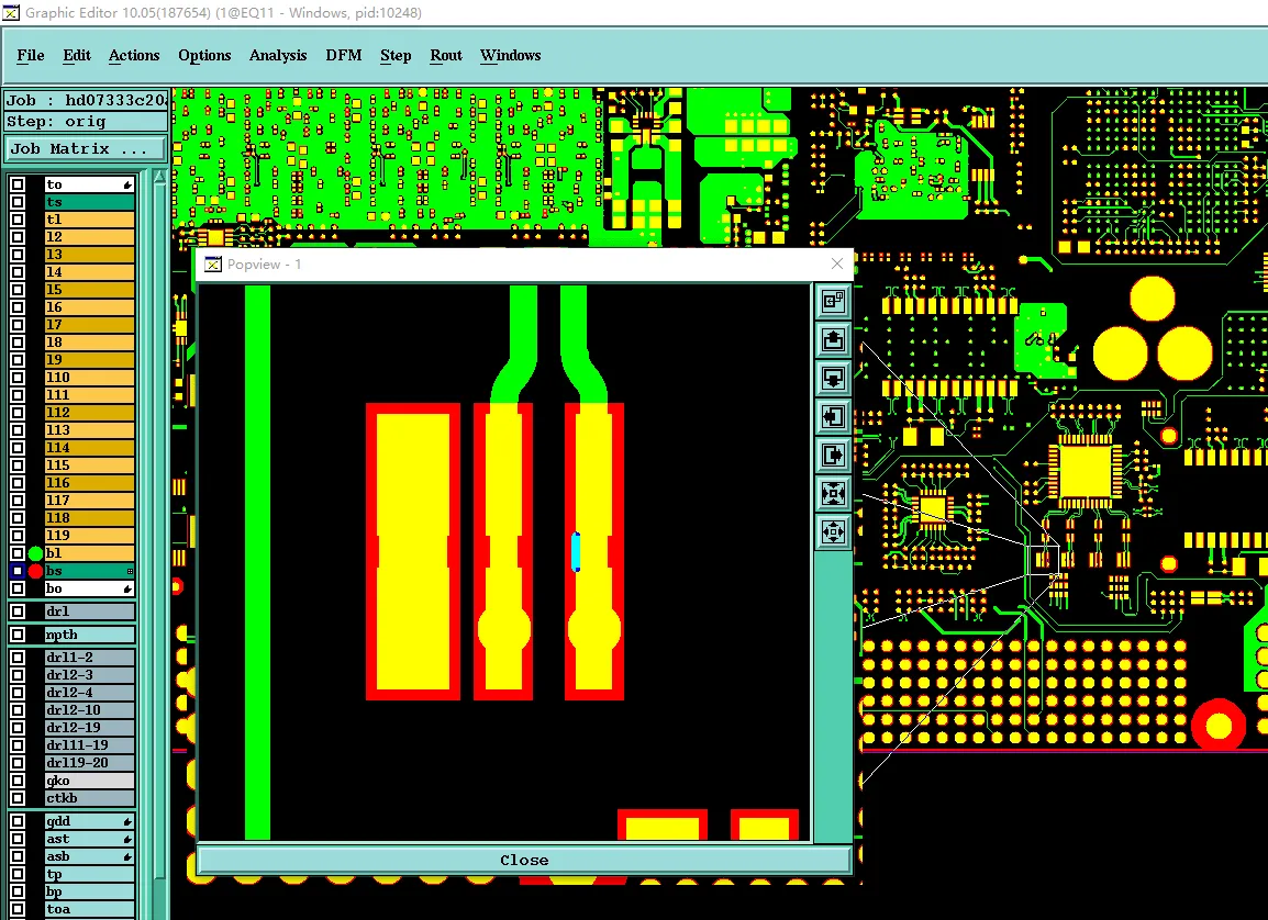
Why Your 20 Layer PCB Fails CAM: Trace Space & Impedance Fixes
How to Resolve Buried Via Stackup and Panelization EQs on TG170 8-Layer PCBs
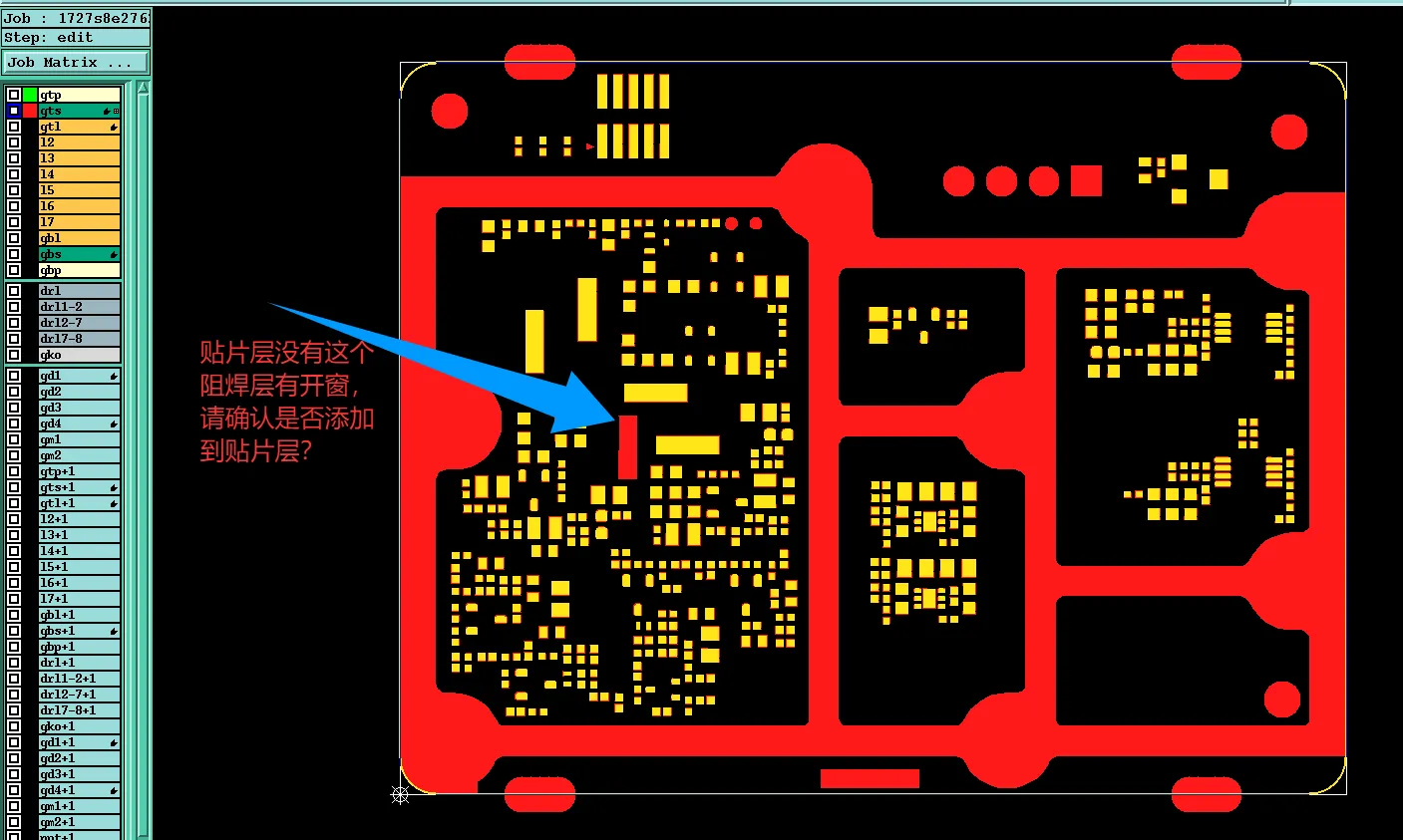
How to Prevent Buried Via Plating and Stackup Mismatch Issues in 8-Layer TG170 PCB
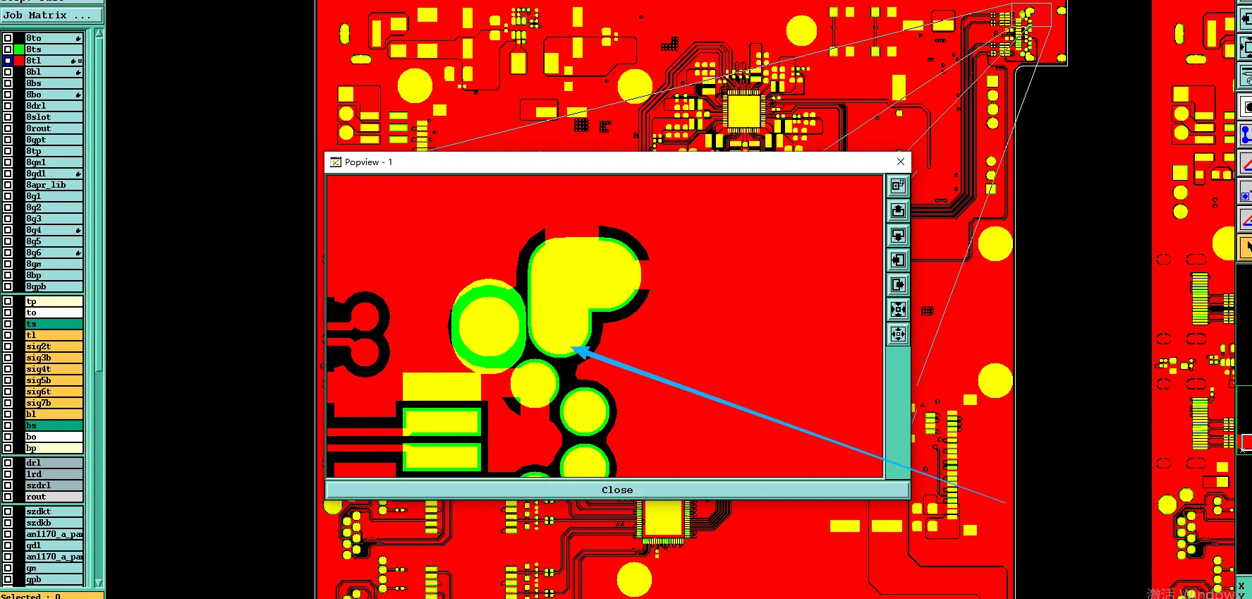
How to Fix Tight Pad Spacing and Impedance EQs in 8-Layer PCB CAM Review
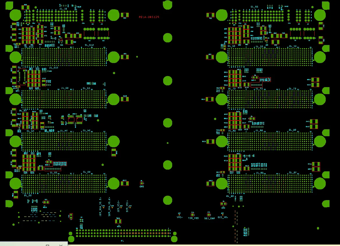
How to Resolve Backdrill, Press-Fit & Copper Balance Issues in 3mm 24-Layer FR4 PCB
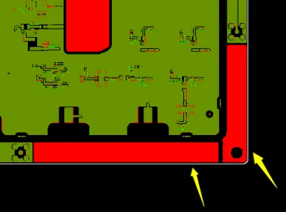
How to Optimize 8-Layer FR4 TG170 PCB Stackup and Panelization for Reliable Manufacturing
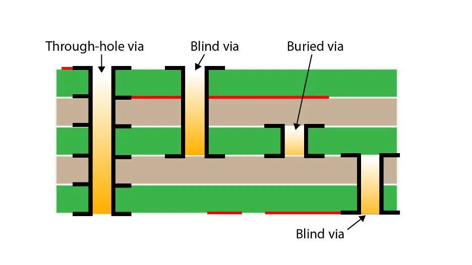
PCB Design Using Blind or Buried Vias Could Lower Fabrication Costs
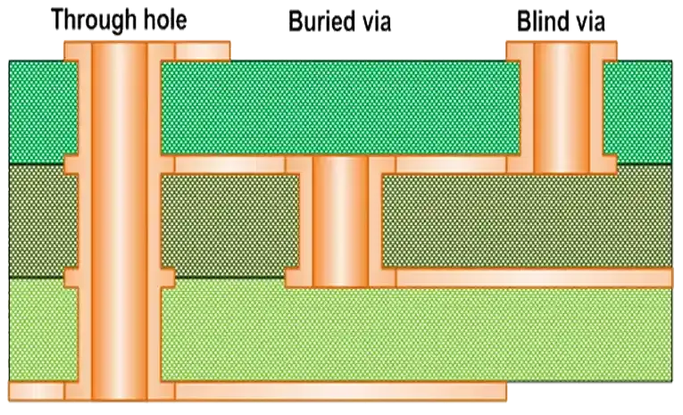
Cost Effective Buried Via Implementation: Balancing Performance and Price
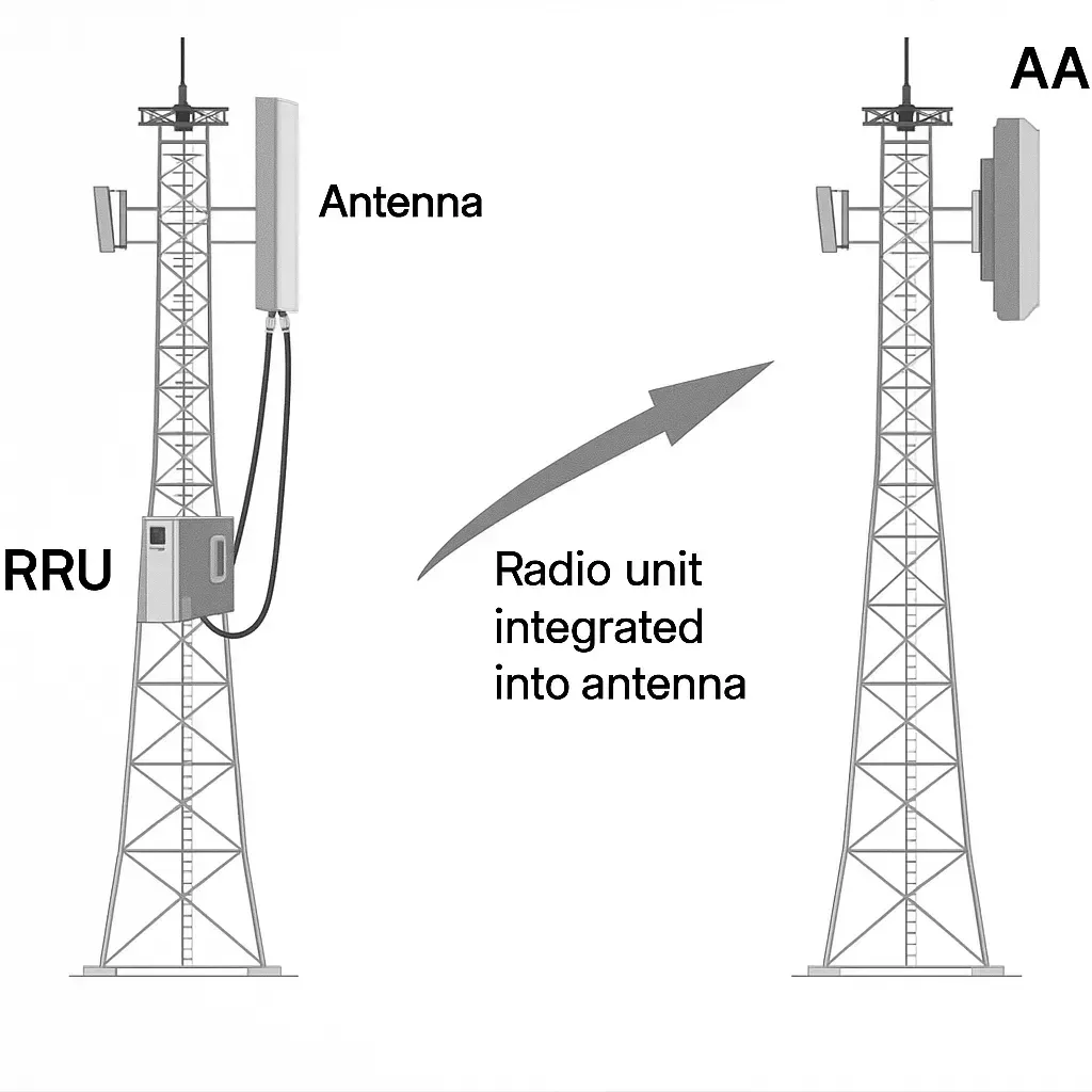
How Are 5G Base Stations Installed?

E Reader PCB Design for IoT Integration: Enabling Wireless Connectivity
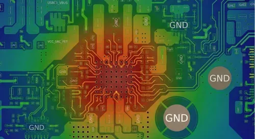
IoT PCB Thermal Management: Preventing Overheating in High Density Designs
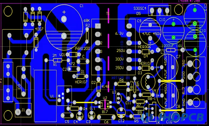
Cost Effective PCB Trace Routing: Strategies for Reducing Manufacturing Costs
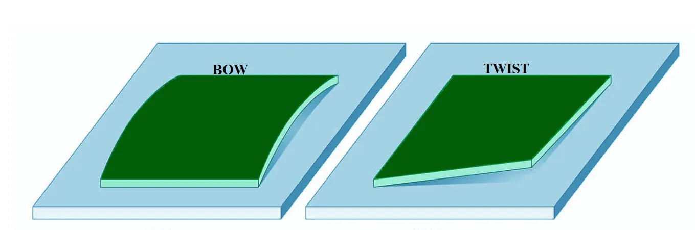
What Role Does PCB Copper Balance Play in PCB Fabrication?

Signal Integrity Secrets: How Thick PCBs Minimize EMI and Crosstalk in High-Speed Circuits