 03:34
03:34
Multilayer PCB
Multilayer PCBs represent a cornerstone of modern electronics design, enabling the creation of compact, high-performance circuits that power everything from smartphones to industrial machinery. These boards consist of multiple layers of conductive copper separated by insulating materials, allowing for intricate routing of signals and power without the space constraints of single or double-layer alternatives. For engineers and designers searching for multilayer PCB solutions, this tag serves as a comprehensive resource, offering insights into their construction, advantages, and implementation strategies. One key benefit of multilayer PCBs is their ability to support higher component density, which is essential for devices requiring complex interconnections while minimizing electromagnetic interference. In practice, this means you can achieve better signal integrity and thermal management, crucial for applications in telecommunications, automotive systems, and medical equipment. When designing a multilayer PCB, focus on layer stackup planning to optimize impedance control and reduce crosstalk; for instance, alternating signal and ground planes can significantly enhance performance. Best practices also include using via structures like blind or buried vias to connect layers efficiently, avoiding common pitfalls such as uneven copper distribution that could lead to warping during fabrication. Professionals often turn to multilayer PCBs for their scalability in prototyping and mass production, where cost-effectiveness hinges on selecting appropriate materials like FR-4 or high-frequency laminates based on the project's demands. This tag compiles articles that delve into these topics, from step-by-step design tutorials to case studies on troubleshooting manufacturing issues. By reviewing the content here, you can gain practical knowledge to refine your projects, whether you're optimizing a new prototype or scaling up for commercial use.
Video Guide


Technical Articles
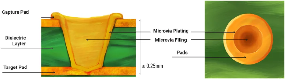
High Aspect Ratio PCBs: Challenges, Solutions, and Advanced Manufacturing Techniques
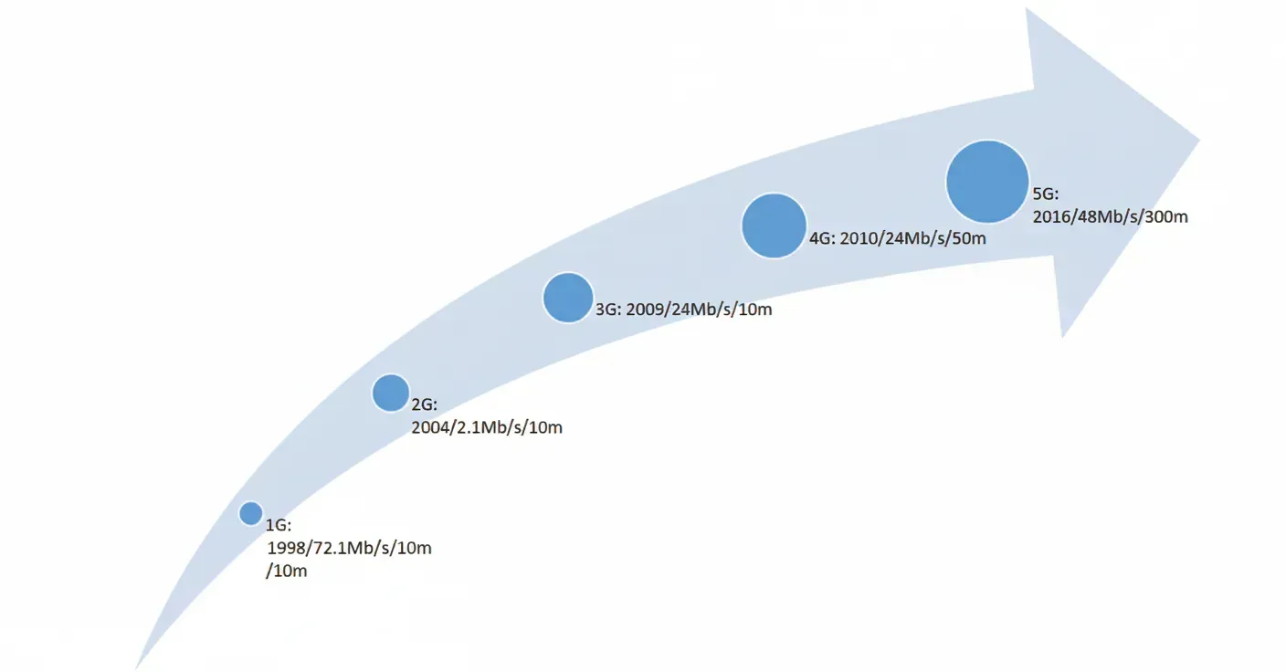
How many wireless systems can a smartphone RF PCB support?
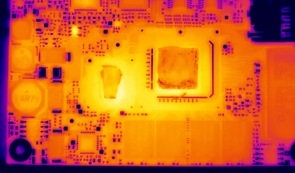
Thermal Runaway: Managing Heat Dissipation in Maximum Sized PCBs
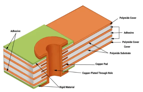
Drill Hole Considerations for PCB DFM: Avoiding Common Manufacturing Errors
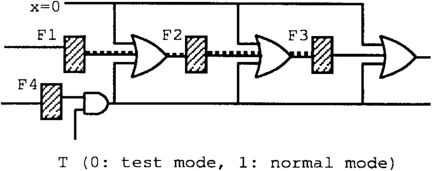
DFT in High Speed PCBs: Addressing Signal Integrity and Testability
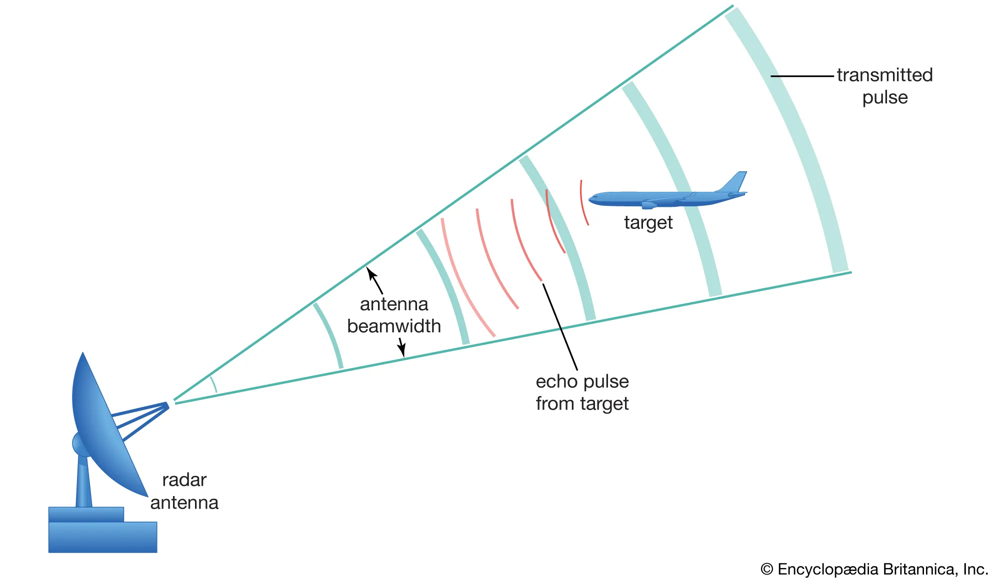
Radar PCB Design for Phased Array Antennas and System Architectures
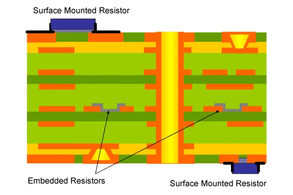
Impedance Control with Buried Resistors: Taming Signal Reflections in High Frequency PCBs
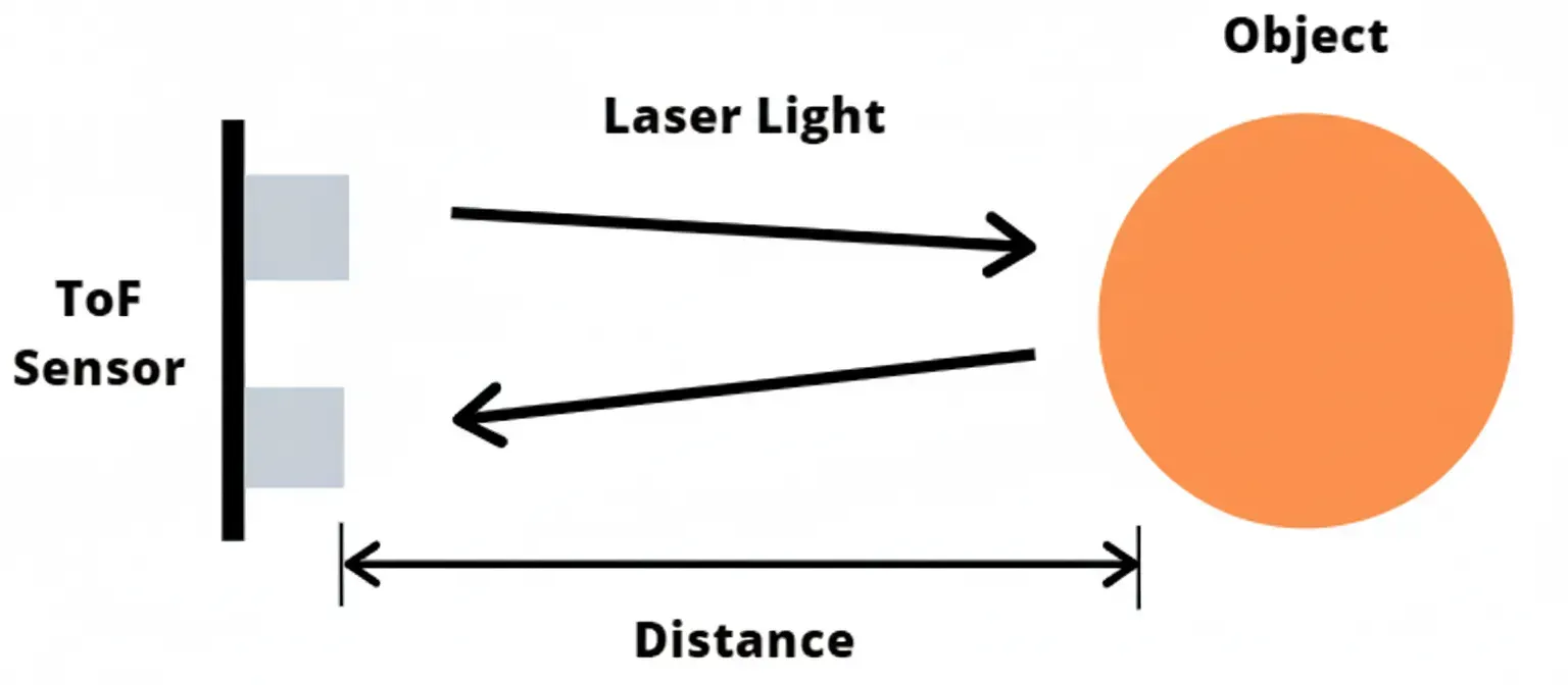
ToF Sensors: Principles, Advantages, Limitations, and Electronics Integration
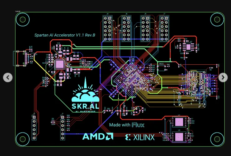
AI Accelerator PCBs for Automotive Applications: Meeting Stringent Safety and Reliability Standards
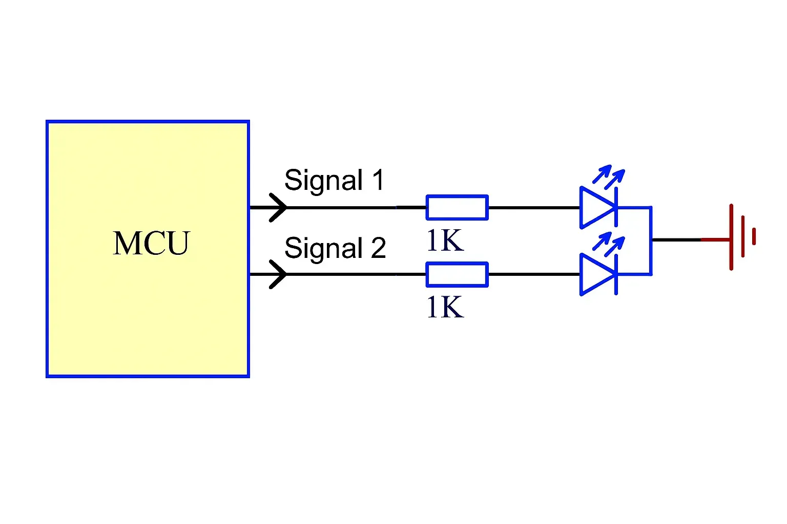
PCB Design for LED Driver Circuits: Operation Types, Power Configurations, and Microcontroller Integration
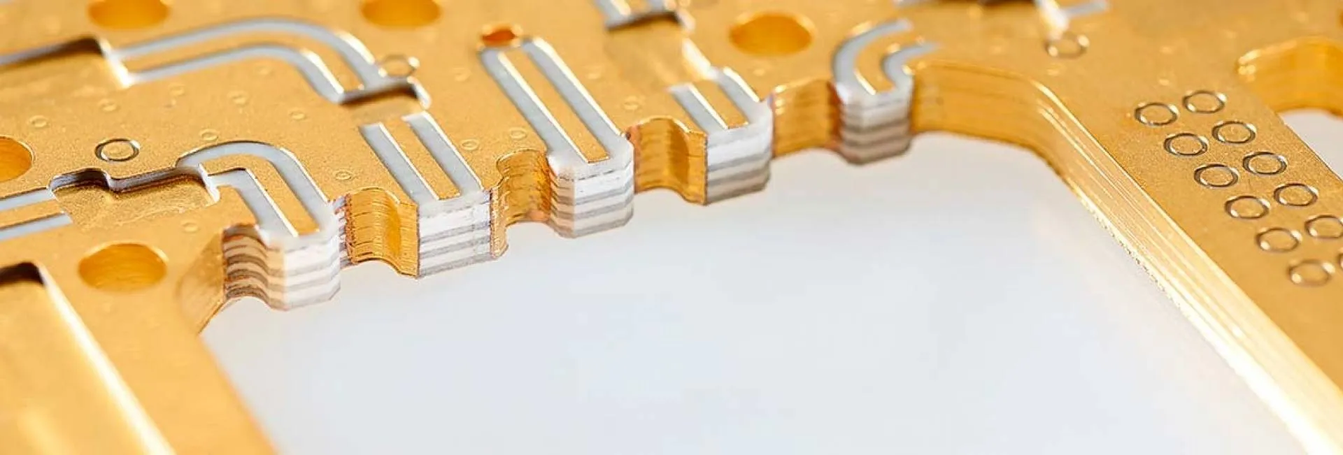
Exploring the Benefits of Multi Layer PTFE PCBs for Complex Designs

How to Design a Multi Layer PCB for Infotainment Systems

WiMAX and Wi-Fi: Technical Differences
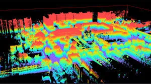
What Is SLAM and Its Main Applications
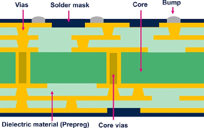
Cost-Effective PCB Solutions: Exploring the Benefits of Organic Substrates

Advanced PCB Stack Up Design for Telecommunication Base Stations: Optimizing Performance and Reliability

LED Display Applications Overview
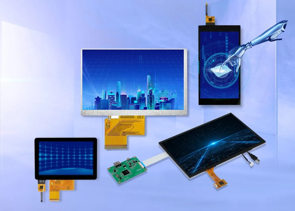
LED Display Control System PCB Design and Manufacturing: Power, Interfaces, and Signal Integrity

Visual SLAM: Current Research Status