 00:49
00:49
PCB Layout Errors
Understanding PCB layout errors is crucial for anyone involved in electronics design, as these mistakes can lead to malfunctioning circuits, increased production costs, and reliability issues in final products. The PCB Layout Errors tag on this blog serves as a comprehensive resource dedicated to identifying, analyzing, and preventing common pitfalls in printed circuit board design. Whether you are a novice engineer troubleshooting your first prototype or an experienced professional optimizing complex multilayer boards, this collection of articles addresses the real-world challenges that arise during the layout phase. By exploring these topics, you gain insights into how seemingly minor oversights, such as improper trace routing or inadequate grounding, can cascade into significant problems like signal interference or thermal failures. One of the primary benefits of delving into PCB layout errors is learning actionable strategies to enhance your design process. For instance, articles under this tag often highlight best practices like adhering to design rule checks (DRC) to catch violations early, implementing proper component placement to minimize noise, and using simulation tools to predict potential issues before fabrication. These practical tips are drawn from industry experiences and case studies, helping you avoid costly revisions and improve overall board performance. Common errors discussed include via placement mistakes, impedance mismatches, and power distribution flaws, each explained with clear examples and corrective measures. This knowledge not only aids in debugging existing designs but also empowers you to adopt preventive habits that streamline future projects. For those seeking to deepen their expertise, the articles linked here provide detailed breakdowns of specific error types, complete with diagrams and step-by-step guidance. By applying these insights, designers can achieve more robust and efficient PCBs, ultimately contributing to successful electronic systems in fields ranging from consumer gadgets to industrial automation.
Video Guide
-
00:49
Technical Articles

Preventing Tombstoning and Cold Solder Joints in 0603-and-Smaller SMT Chips with Thermal Relief
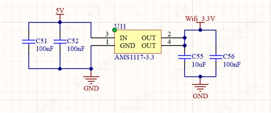
PCB Design Essentials for LDO Power Supplies
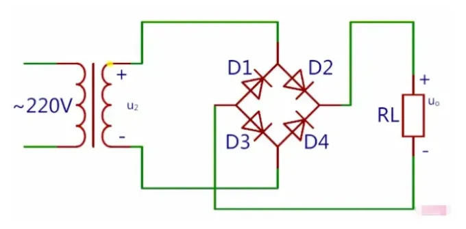
Bridge Rectifier Operation: Current Paths, Waveforms, and Practical Design Notes
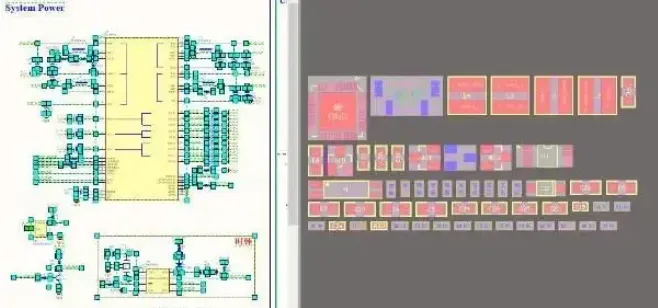
Boost PCB Design Efficiency with Interactive Cross-Probing and Modular Placement
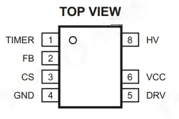
AC-DC Power Conversion: Circuit Methods, HFC0500 Example, and PCB Layout Rules
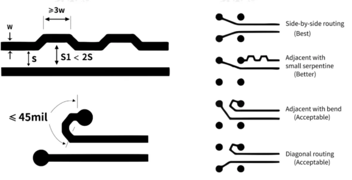
PCB Layout and Routing Requirements for a DP 1.4 Interface
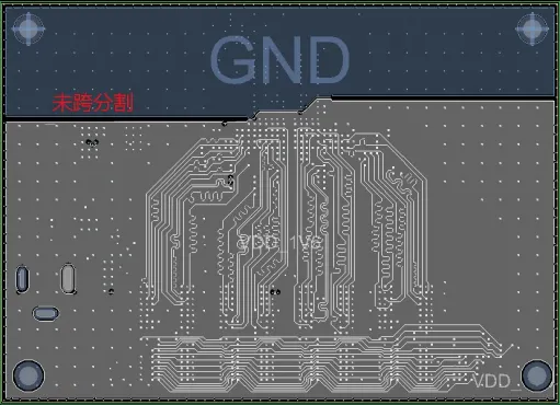
PCB Design Pitfalls: Layout, Routing, and Fabrication Details That Can Fail a Board
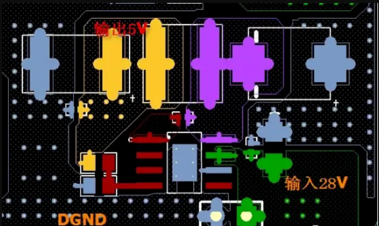
DC-DC Power-Module PCB Layout: 10 Rules That Usually Decide the Result
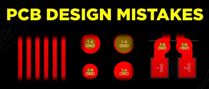
The Ten Most Common Beginner Mistakes in PCB Layout

Enhancing Audio Quality: An Electrical Engineer's Guide to DSP Noise Cancellation

Simple Techniques for Accurate PCB Drilling at Home
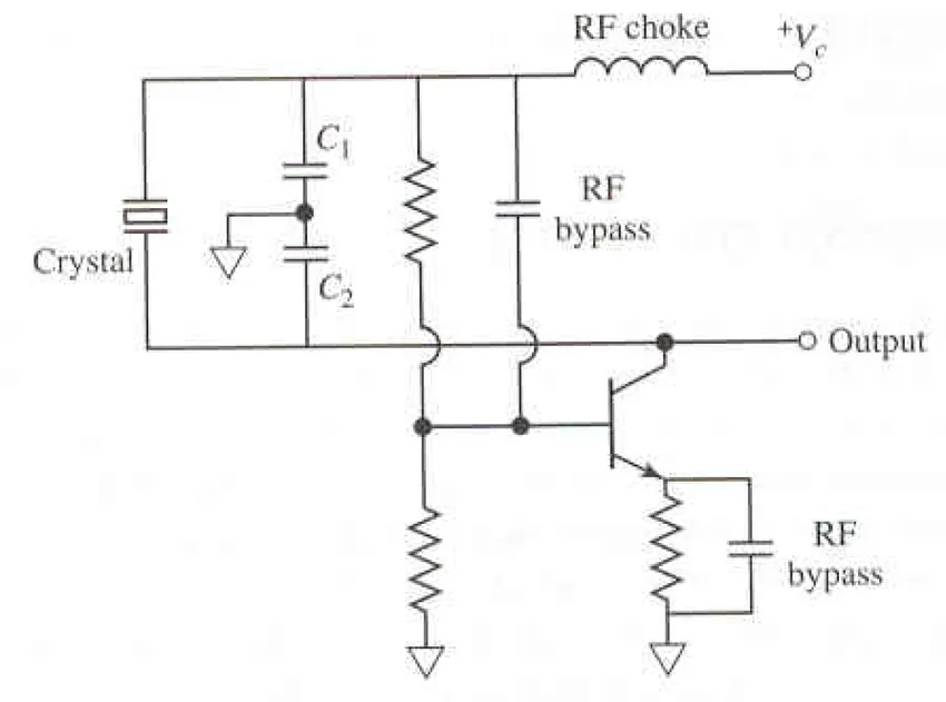
Crystal Oscillator Startup Issues? Debugging Tips for PCB Designers
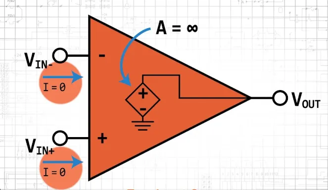
Common Op Amp Circuit Properties
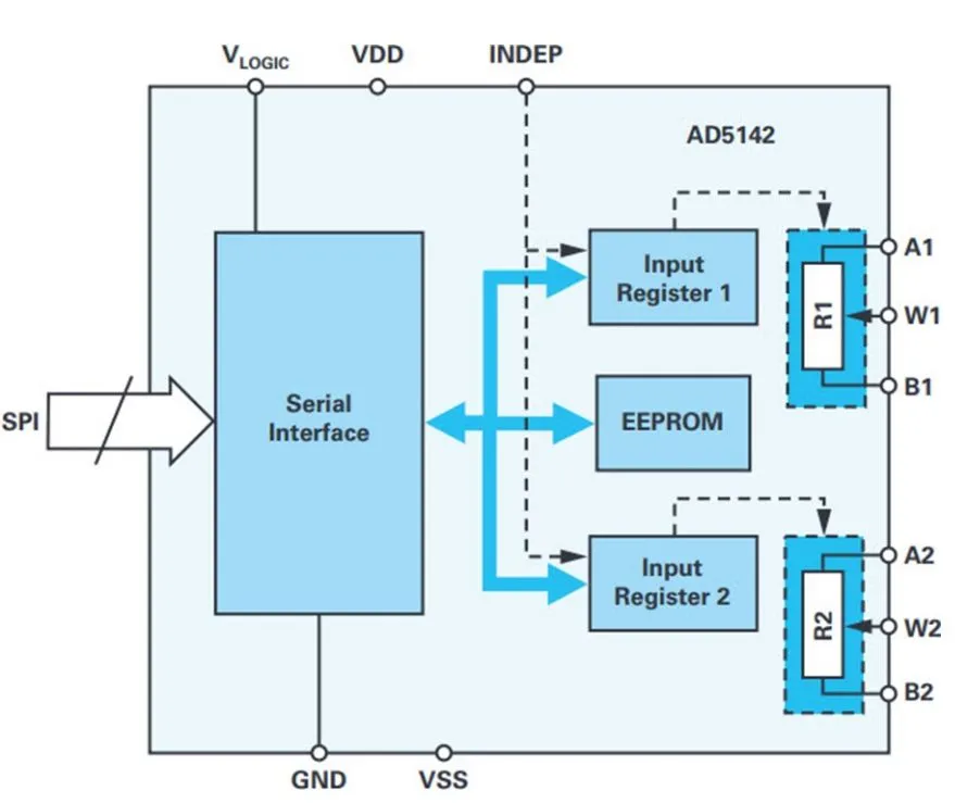
Simple Programmable Wien Bridge Oscillator Design Using Digital Potentiometers
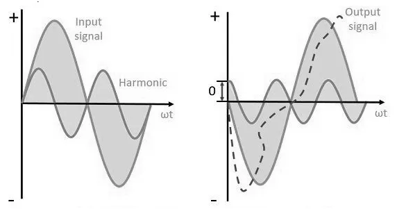
Types of Amplifier Distortion and How to Reduce Them
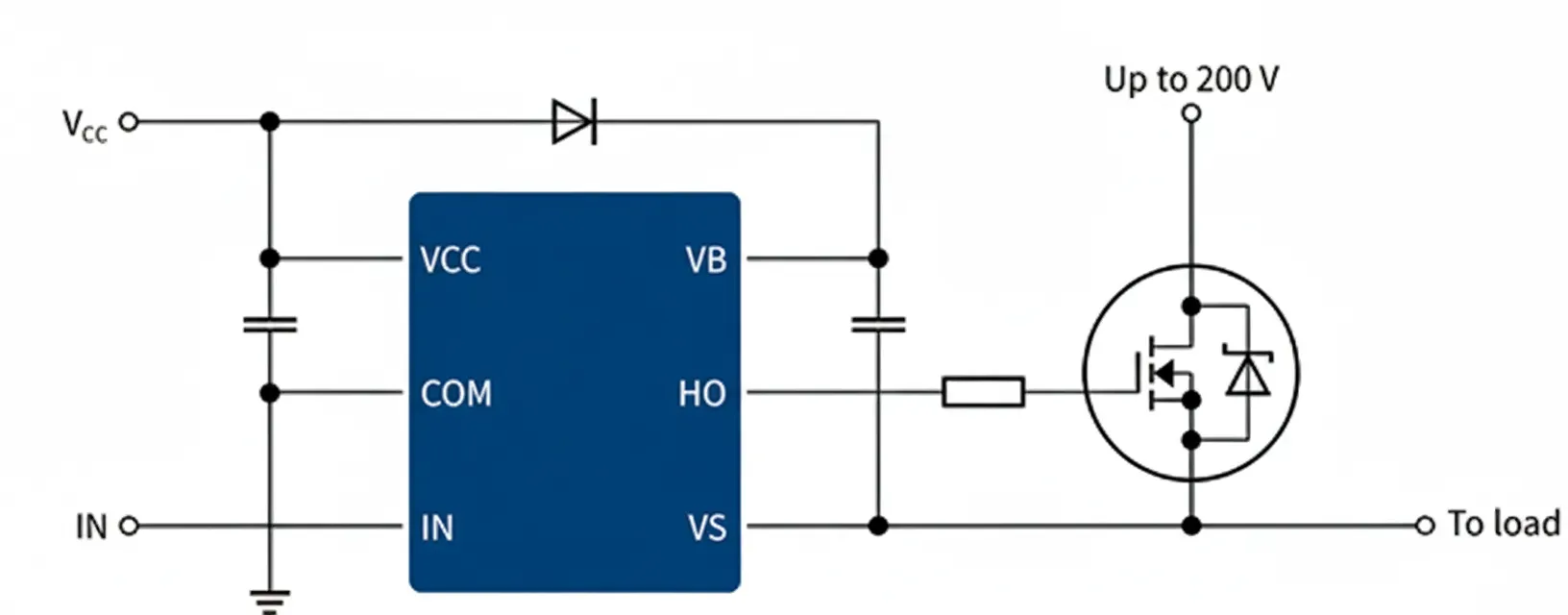
Common MOSFET Circuits for Power Switching
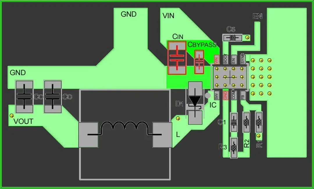
DC-DC Switching Power Supply Design Principles
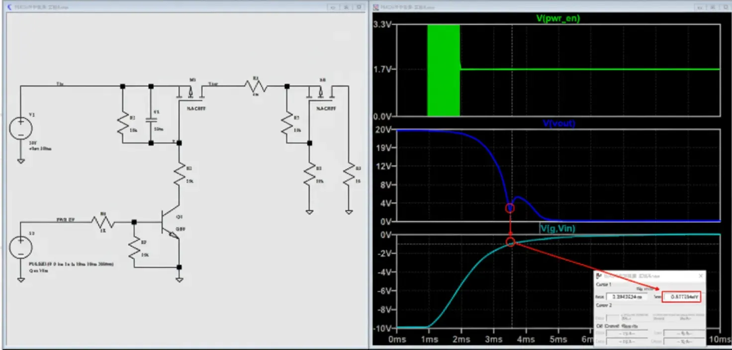
PMOS Switch Simulation Circuit Analysis
Key PCB Layout Guidelines for Buck Converters