Solder Mask Misalignment
Solder mask misalignment is a common issue in printed circuit board (PCB) fabrication that can lead to functional failures, reduced reliability, and increased production costs. This tag page gathers essential resources and articles focused on identifying, preventing, and correcting solder mask misalignment, helping engineers, designers, and manufacturers address this challenge effectively. By exploring the content here, you can gain a deeper understanding of how misalignment occurs during the masking process, often due to factors like thermal expansion, improper registration, or equipment calibration errors. For those searching for solutions to solder mask misalignment, the articles under this tag offer practical insights into diagnostic techniques, such as visual inspections using magnification tools or automated optical inspection (AOI) systems. You'll find discussions on root causes, including substrate material variations and process tolerances, along with best practices for achieving precise alignment. These include optimizing artwork preparation, selecting appropriate solder mask materials, and implementing quality control measures in the manufacturing workflow to minimize defects. Professionals in PCB assembly will appreciate the actionable advice on rework strategies, such as selective mask removal or redesigning pad layouts to accommodate potential shifts. Case studies highlight real-world applications, demonstrating how resolving misalignment has improved yield rates and product performance in high-stakes industries like automotive and consumer electronics. As you delve into these resources, you'll discover strategies that not only fix immediate problems but also enhance overall design robustness for future projects. This collection serves as a valuable reference for anyone aiming to elevate their PCB production standards and avoid costly errors.
Technical Articles

Why the Solder Mask Bridge Disappears Even When There Is a Gap Between Pads
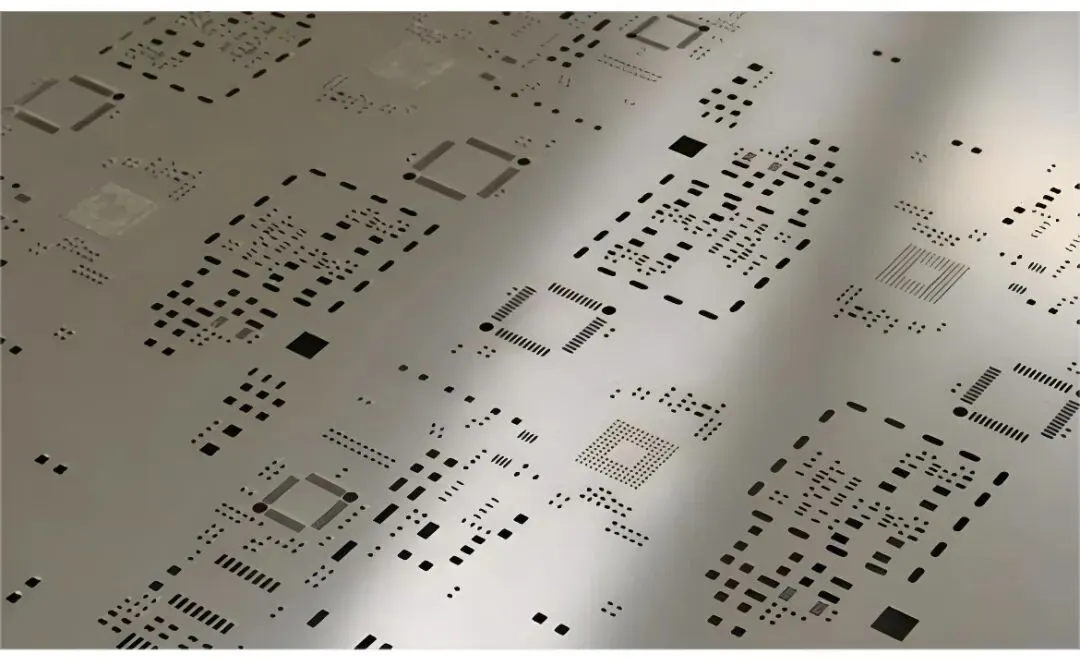
Solder Mask vs. Paste Mask: Why a 0.1 mm Error Can Scrap an Entire PCB Batch

PCB Solder Mask Openings and Solder Mask Dams: Design Intent and Manufacturing Considerations
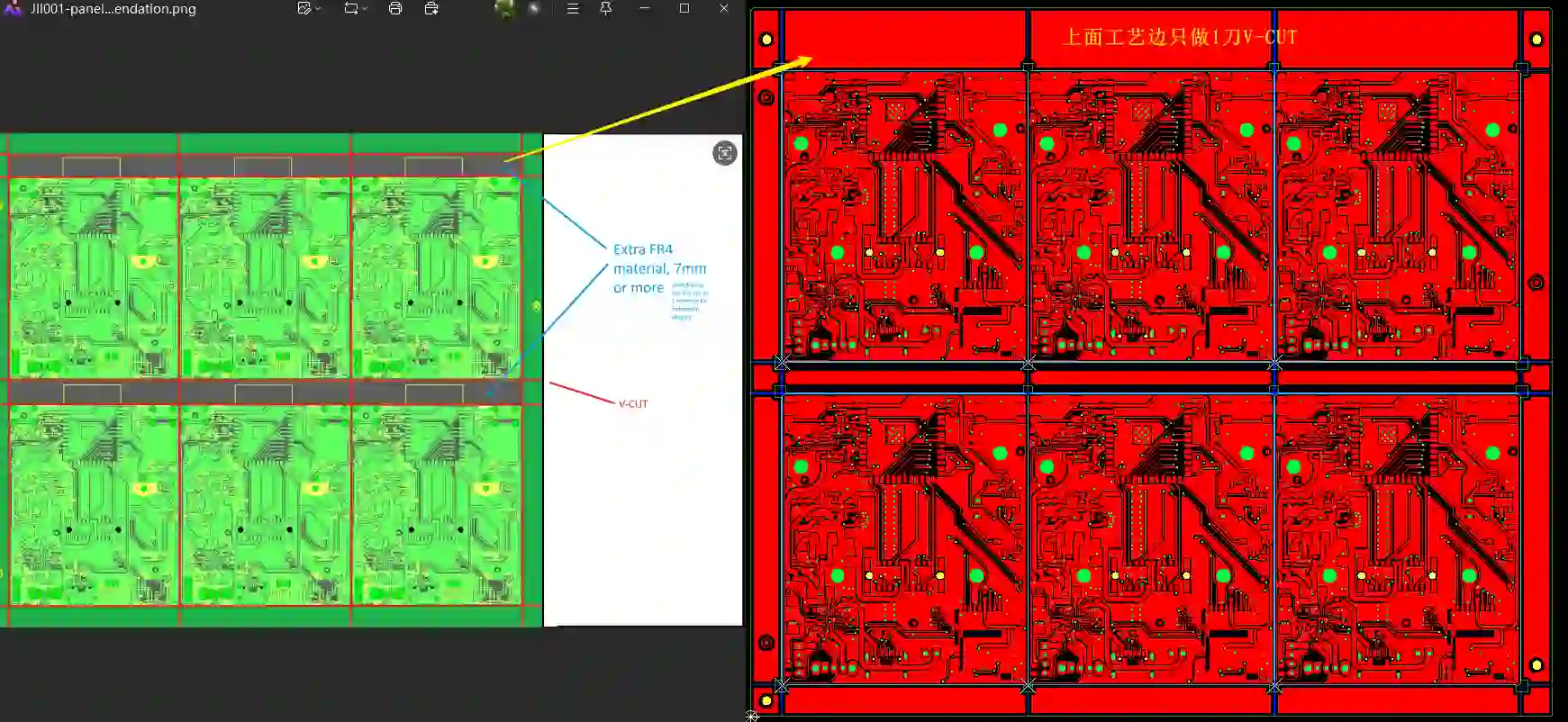
How to Solve 2-Layer PCB CAM Issues Before Manufacturing
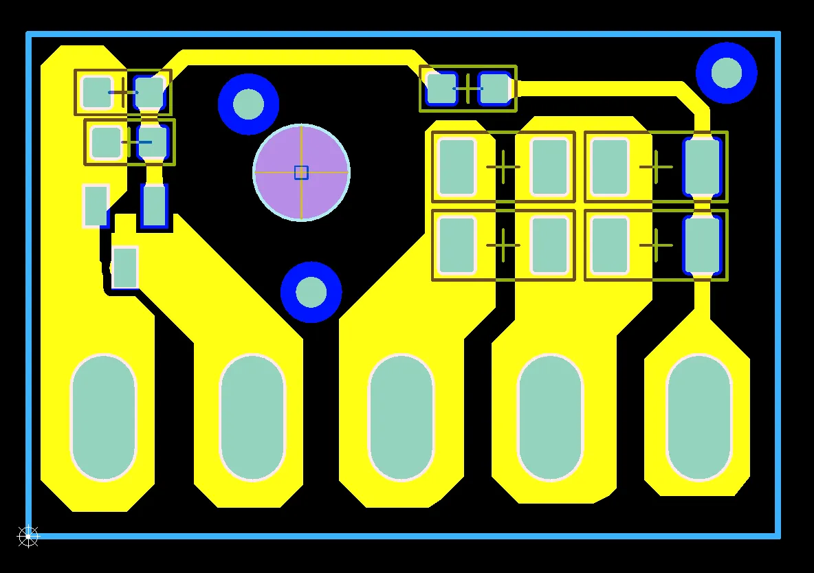
Common 1 Layer FR4 PCB EQ Issues: How Manufacturers Review Gerber Files
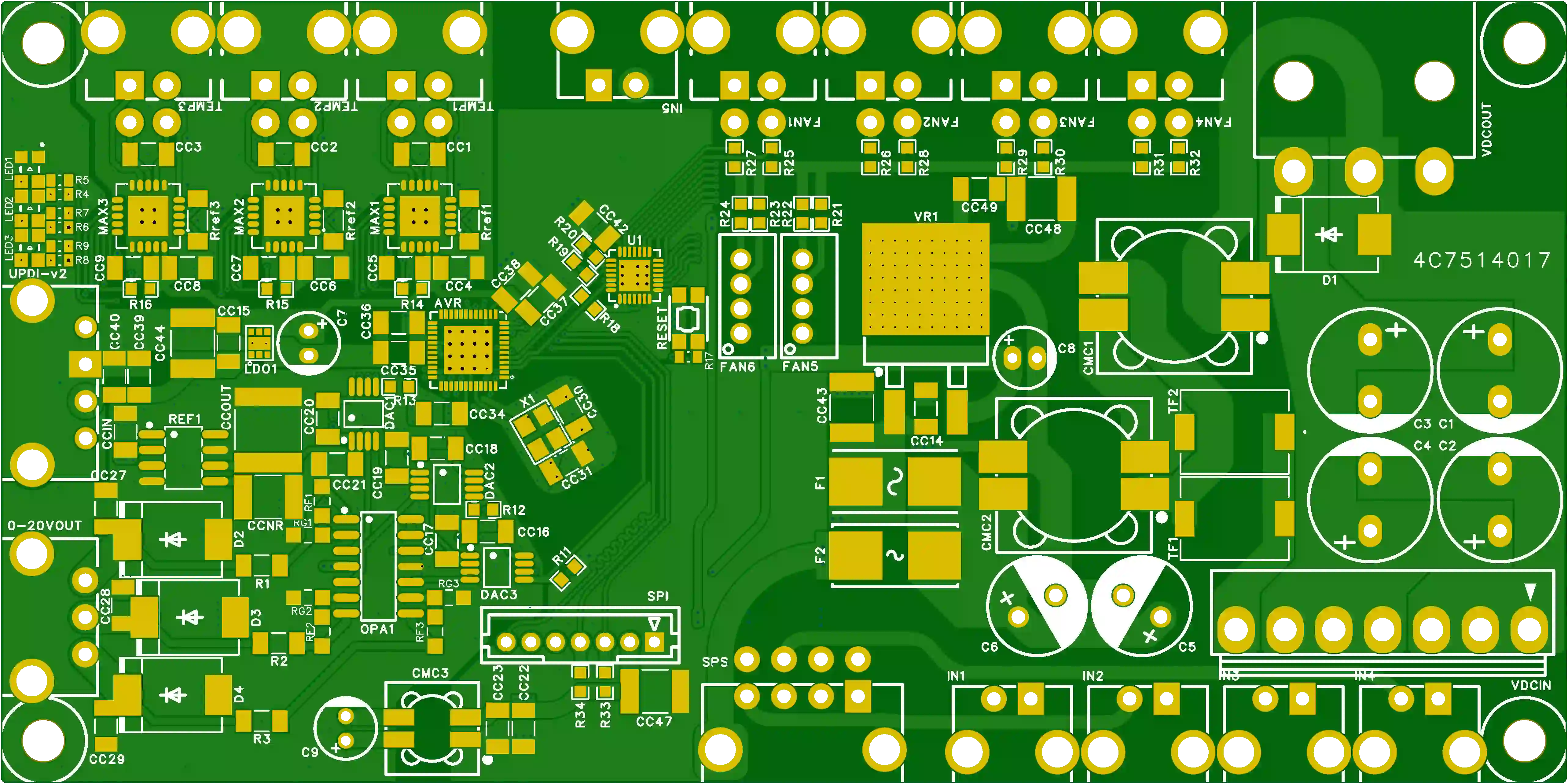
How Conflicting Via Data and Soldermask Definitions Triggered CAM Review in a 4-Layer HDI PCB
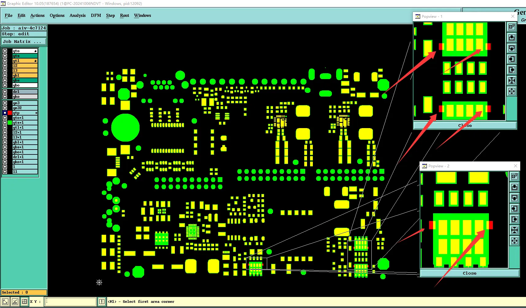
Solder Mask vs. Paste Mask: Perfecting Your Opening Design
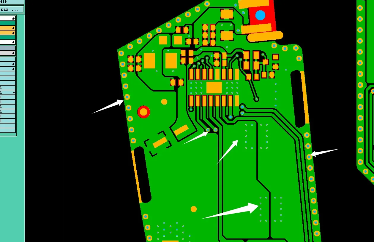
How We Resolved PCB Solder Mask Opening Design Conflicts in a 2-Layer FR4 PCB
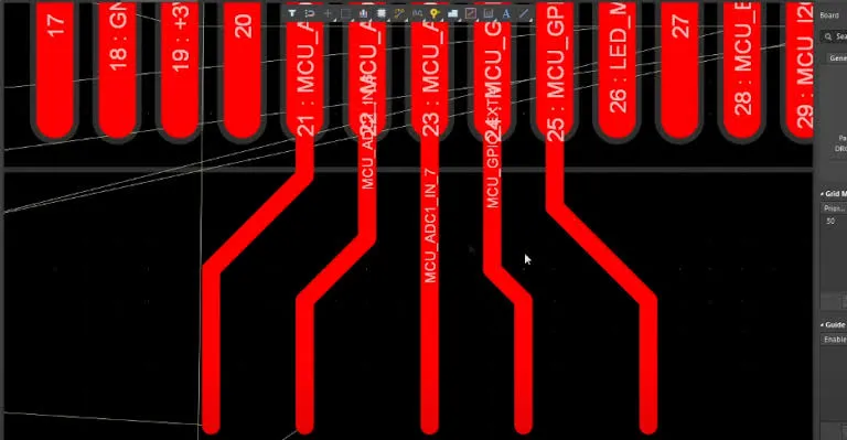
Common HDI Gerber Design Mistakes Found During CAM Review
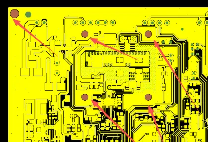
How to Fix 2 Layer FR4 PCB Design Errors During CAM Review
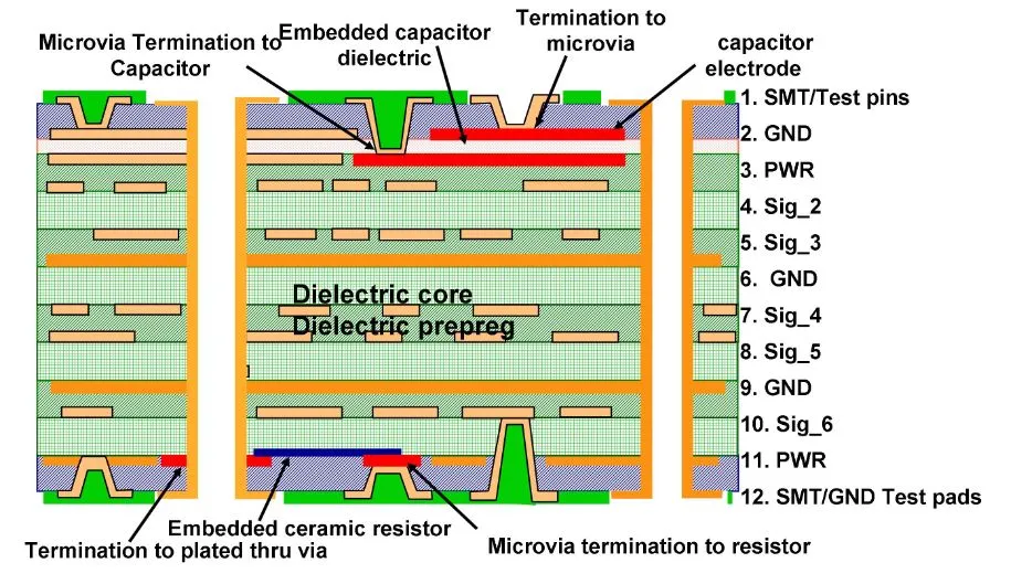
How PCB Manufacturers Improve Solder Mask Yield in HDI Production
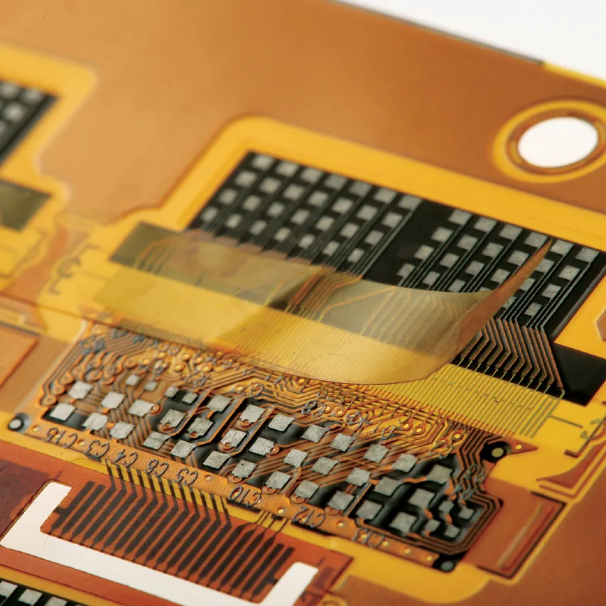
FPC Tape: Why Flush Edges Cause Adhesive Overflow

How Do FPC Factories Compensate Coverlay Openings in Practice?
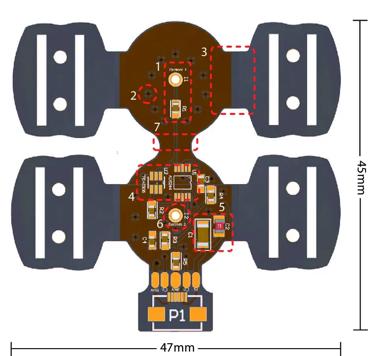
What Happens When FPC Characters Are Placed on or Too Close to Pads
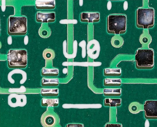
Solder Mask Misalignment Guide: Causes, IPC Standards, and Prevention
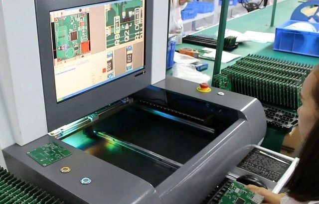
The Impact of Solder Mask on Thick Copper PCBs: Challenges and Solutions

The Impact of Solder Mask on PCB Gold Finger Performance: Best Practices
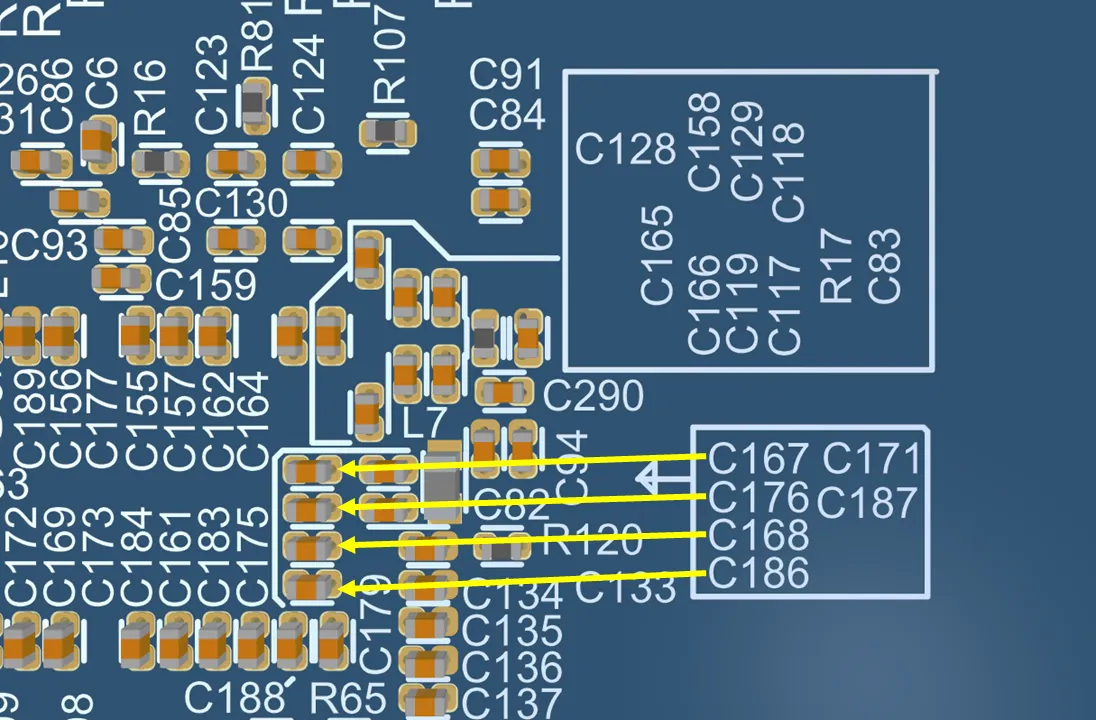
Silkscreen Design Mistakes to Avoid: Ensuring Error Free PCB Assembly