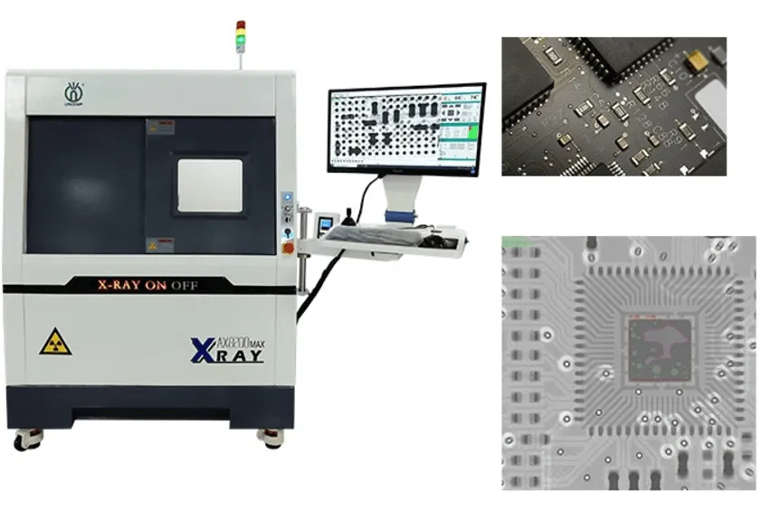
X-Ray Inspection
X-Ray inspection plays a crucial role in the field of printed circuit board (PCB) manufacturing and electronics assembly, offering a non-destructive method to peer inside components and detect hidden defects that traditional visual inspections might miss. This technique utilizes high-energy X-rays to generate detailed images of internal structures, revealing issues such as voids in solder joints, misaligned components, or cracks in multilayer boards. For engineers, quality control specialists, and hobbyists alike, understanding X-Ray inspection is essential for ensuring the reliability and performance of electronic devices, particularly in high-stakes industries like aerospace, automotive, and medical equipment where failure is not an option. In practice, X-Ray inspection systems come in various forms, from 2D radiography for quick scans to advanced 3D computed tomography for comprehensive volumetric analysis. When implementing this technology, start by selecting equipment that matches your production volume and resolution needs; for instance, automated inline systems can integrate seamlessly into assembly lines for real-time defect detection, reducing rework costs and time to market. Best practices include calibrating the system regularly, training operators on image interpretation to distinguish between acceptable variations and critical flaws, and combining X-Ray data with other testing methods like automated optical inspection for a holistic quality assurance approach. By identifying problems early, such as insufficient solder fill or foreign material inclusions, you can prevent costly field failures and enhance overall product durability. This tag on X-Ray inspection gathers in-depth articles that delve into these topics, providing guidance on everything from basic principles to cutting-edge applications. Readers interested in optimizing their inspection processes will find valuable resources here, including case studies on troubleshooting common PCB defects and tips for complying with industry standards like IPC-A-610. Diving into these pieces can equip you with the knowledge to implement effective X-Ray strategies in your own projects.
Technical Articles

Manufacturing Process Study for 0.3 mm Pitch QFN Packages
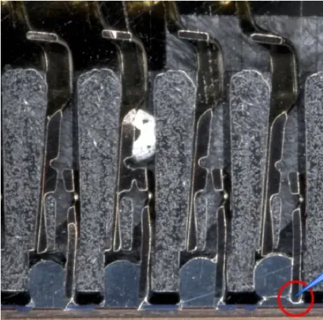
SMT CPU Socket Functional Test Failures: Root Cause and Corrective Action
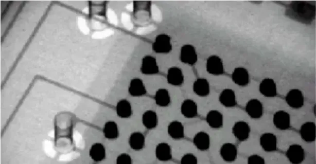
BGA Soldering Defects: A Comprehensive Guide for SMT Process Engineers

Root Cause Analysis and Corrective Actions for a 76% Open-Solder Rate on Recycled BGA Devices
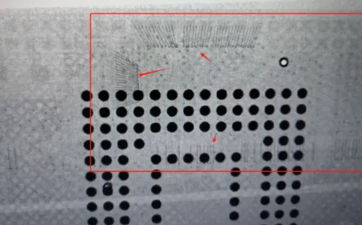
X-Ray Inspection of eMMC BGA: Solder Ball Assessment and an Unexpected Finding
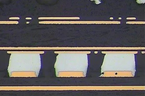
14 Common PCBA Test Methods

Compatible Pad Design and Soldering Reliability Validation for FCQFN and WLCSP Packages
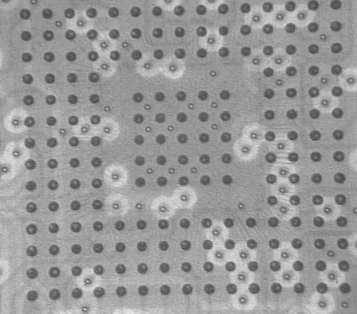
Ensuring PCB Reliability: A Deep Dive into Solder Joint Voids
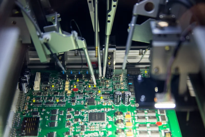
Challenges in using FPT
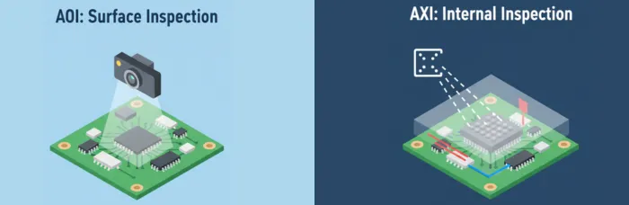
Visual Inspection Vs. Automated X Ray: Choosing the Right PCB Inspection Method
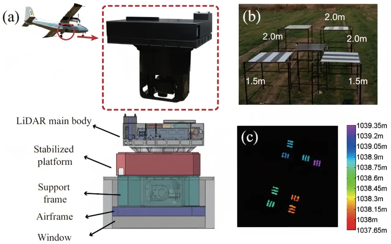
Principles of Ghost Imaging
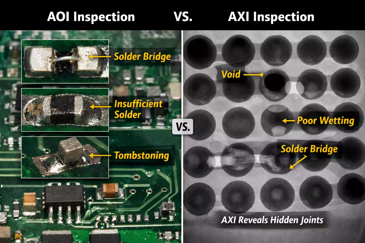
AOI vs. X Ray: Choosing the Right Solder Joint Inspection Method for Your PCB
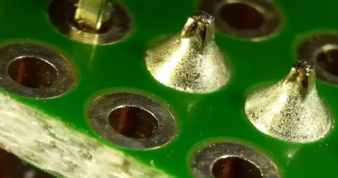
The Ultimate Guide to Solder Joint Inspection: Techniques, Tools, and Best Practices
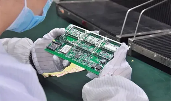
Top 7 PCB Testing Methods to Guarantee Quality and Reliability
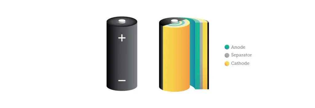
EV Battery Packs: Role and Li-ion Manufacturing
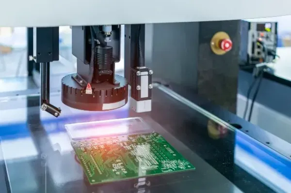
Selecting the Right PCB Inspection Equipment: A Guide to AOI, X Ray, and Flying Probe Testing
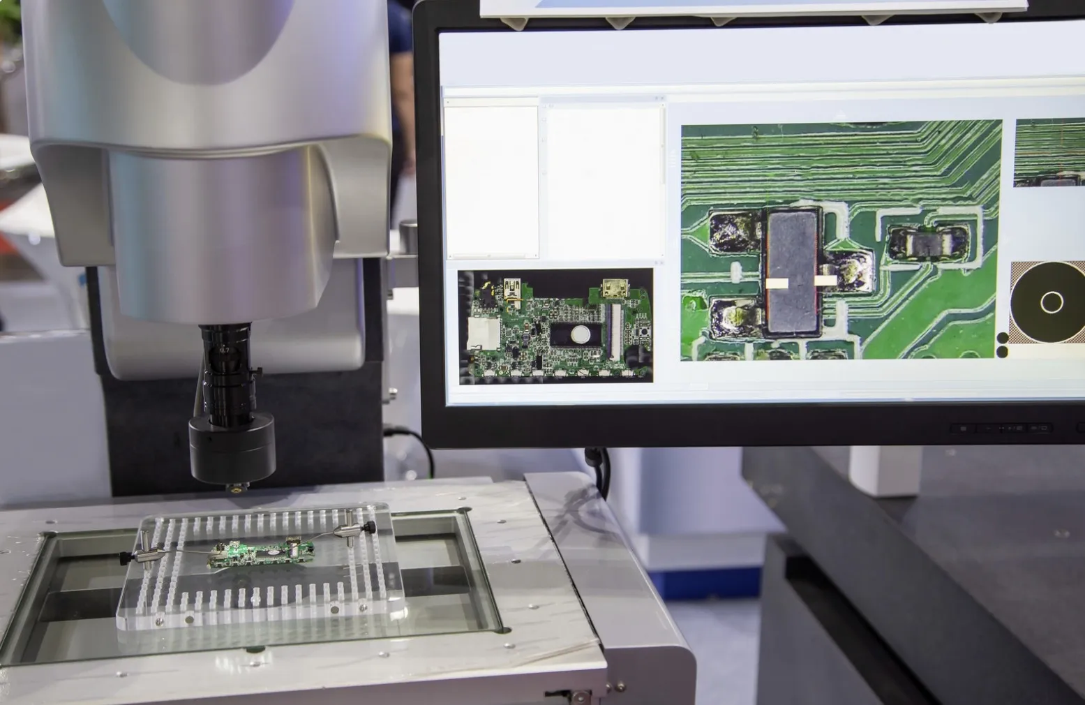
The PCB Imaging: Challenges Manufacturers Face With PCB Inspection
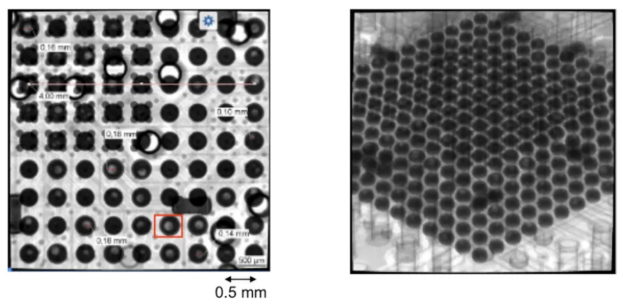
Troubleshooting PCB Assembly with X Ray: A Practical Guide for Engineers