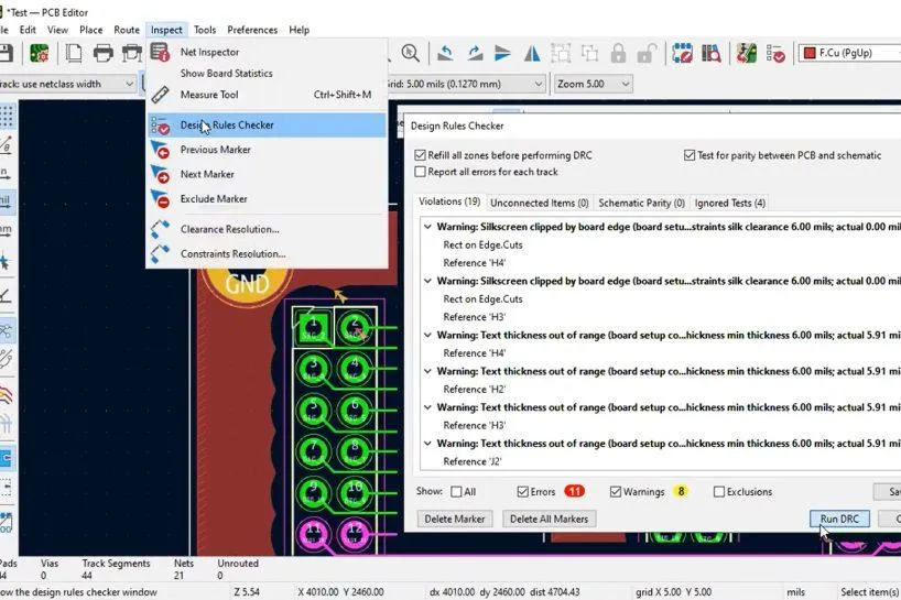
 01:02
01:02
Component Footprints
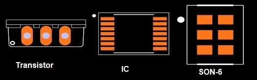
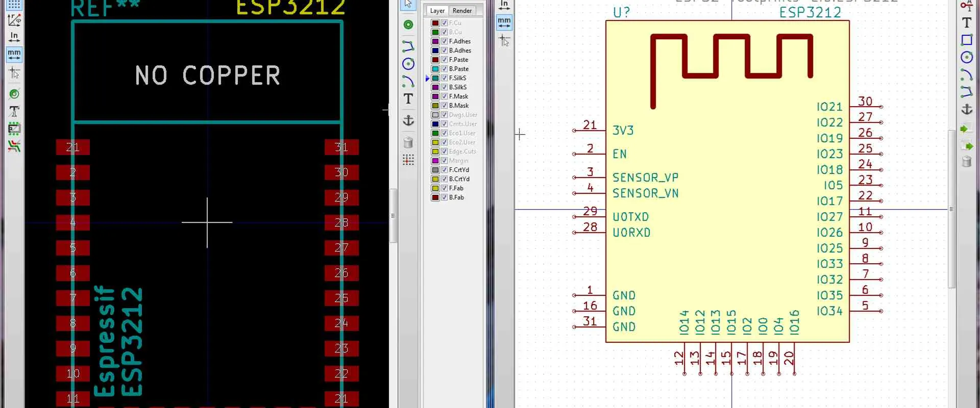
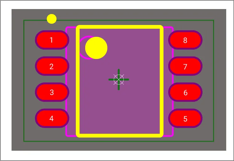
Component footprints form the foundational blueprint for placing and soldering electronic parts onto printed circuit boards (PCBs). In the realm of PCB design, a component footprint refers to the precise pattern of pads, holes, and outlines that correspond to a specific device's physical dimensions, pin layout, and mounting requirements. This tag, Component Footprints, gathers articles that delve into the intricacies of creating, selecting, and optimizing these essential elements, helping engineers and hobbyists ensure reliable assembly and functionality in their projects. Understanding component footprints is crucial for avoiding common pitfalls such as misalignment, poor solder joints, or electrical shorts that can derail a prototype or production run. For instance, when designing for surface-mount devices (SMDs) like resistors or integrated circuits, adhering to standards from organizations like IPC ensures compatibility with automated assembly processes. Practical applications include using CAD software tools such as KiCad or Eagle to generate custom footprints, verifying them against manufacturer datasheets, and incorporating thermal considerations for high-power components. Best practices emphasize starting with verified library footprints to save time, performing design rule checks (DRC) to catch errors early, and iterating based on real-world testing to refine pad sizes and shapes for better yield rates. Whether you are troubleshooting footprint-related issues in an existing design or seeking guidance on adapting footprints for unique form factors, the resources here provide step-by-step insights tailored to various experience levels. Browsing through these articles can equip you with the knowledge to enhance your PCB layouts, from basic through-hole components to advanced ball grid arrays (BGAs), ultimately leading to more robust and efficient electronic systems.
Video Guide
-
01:02
Technical Articles
Why a Small Footprint-Origin Shift Moves Every Pick-and-Place Coordinate
Practical Pad Naming Conventions in PCB Layout Libraries
Boost PCB Design Efficiency with Interactive Cross-Probing and Modular Placement
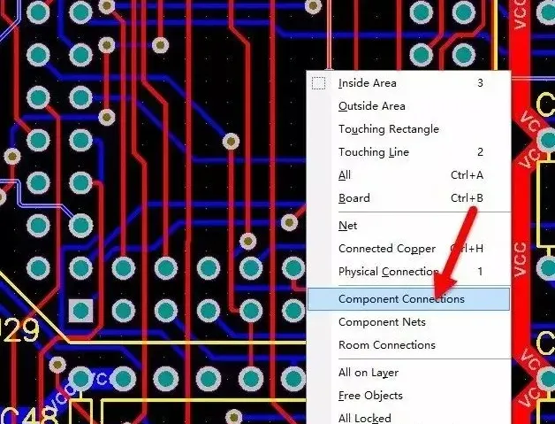
Selecting and Unrouting Nets Associated with a Component in PCB Layout
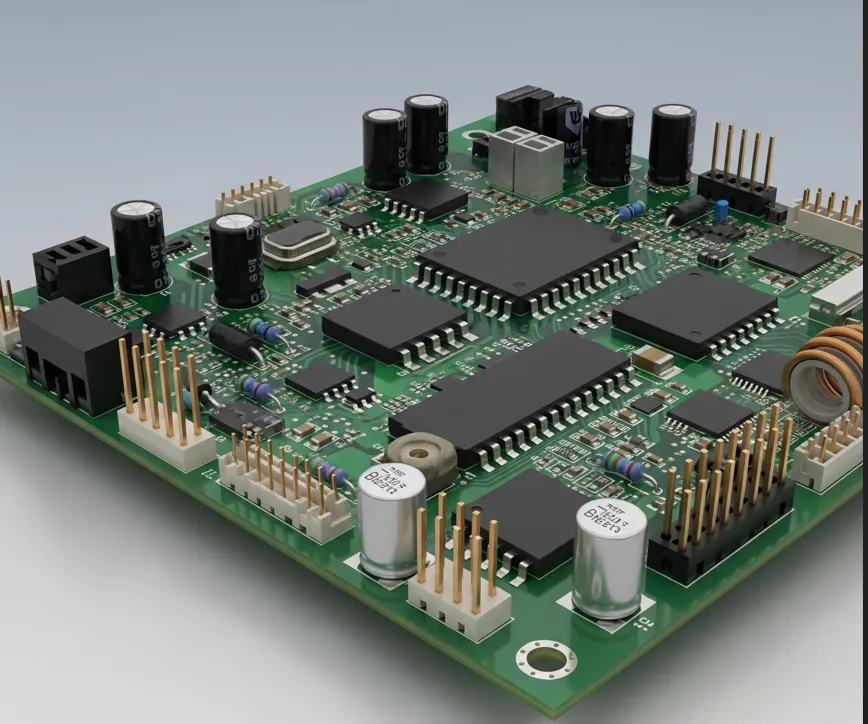
Mastering KiCad 3D Models: Linking Footprints, Embedding Files, Ray Tracing, and CLI Exports
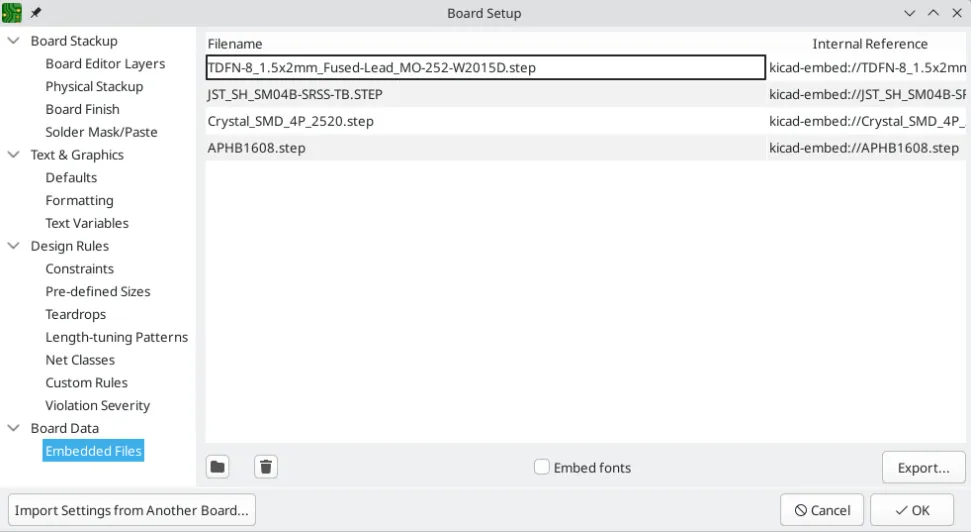
File Embedding Explained (Part 1): Embedding 3D Models in PCB Footprints
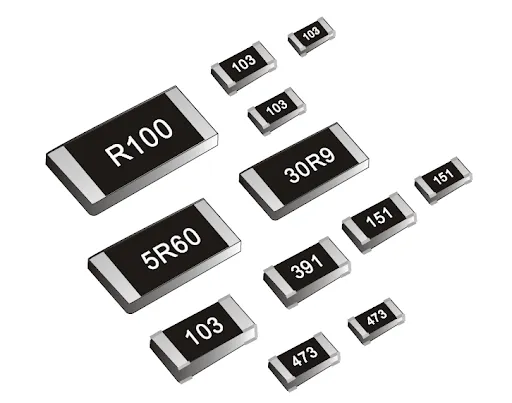
SMD Resistor Codes and Resistance Value Calculations
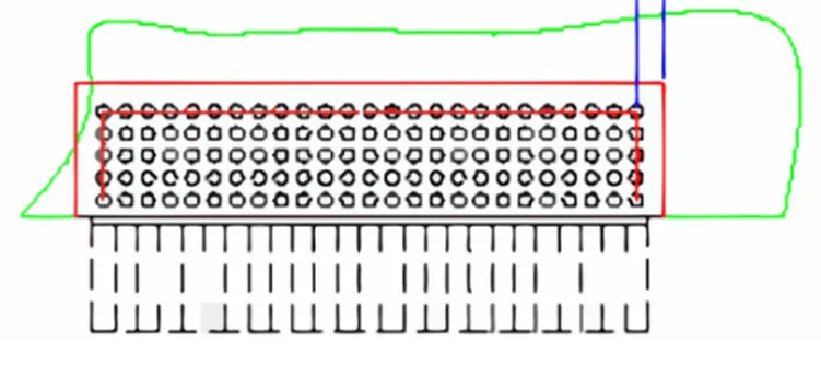
Why Moving a Component Only 1 mm from a Press-Fit Connector Still Causes Assembly Interference
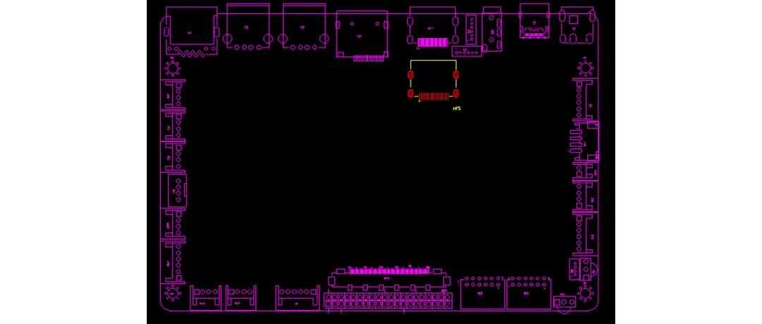
Why a Small Shift in Footprint Origin Moves Every Pick-and-Place Coordinate
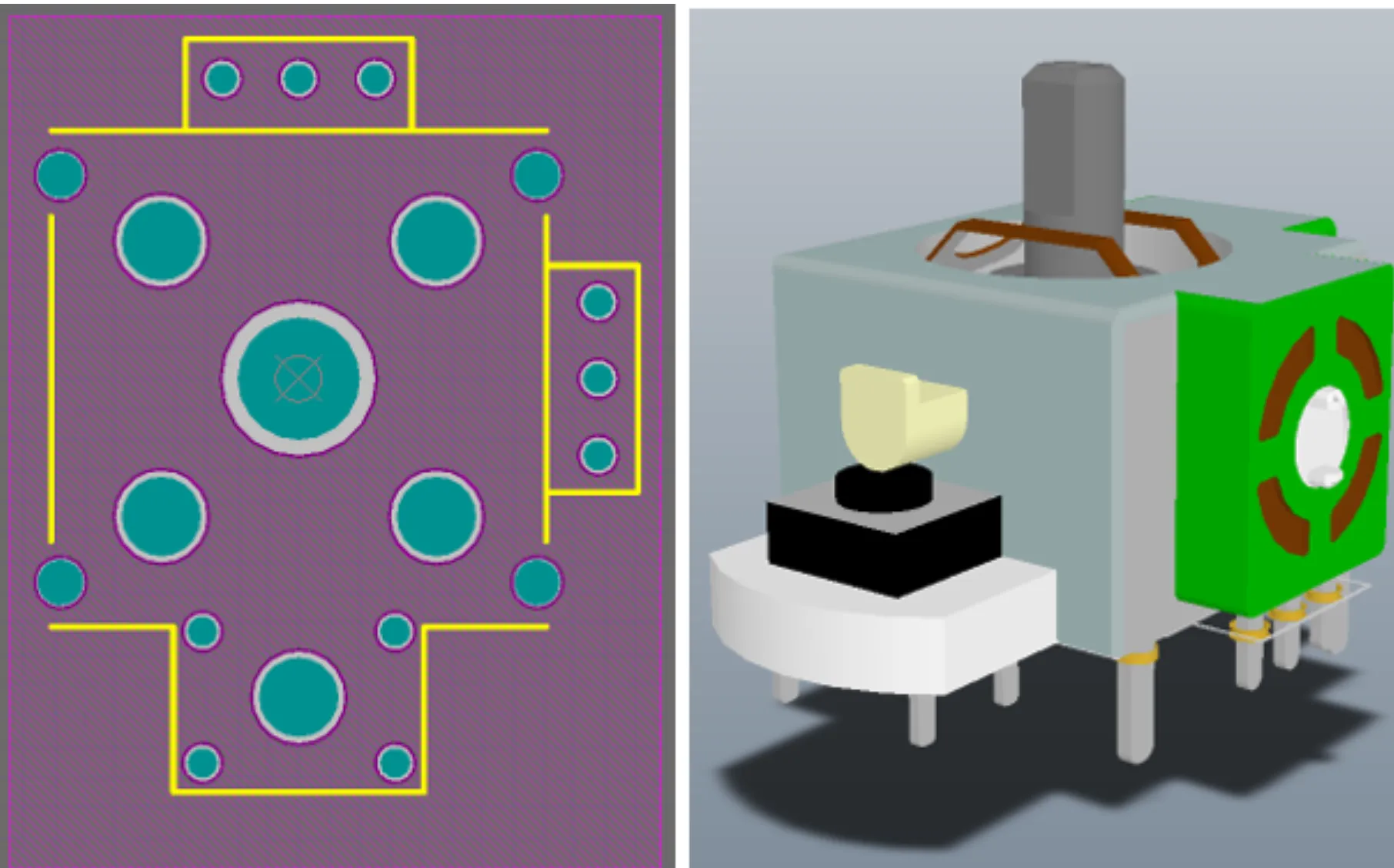
Creating Custom Component Footprints: When and How to Break the Rules
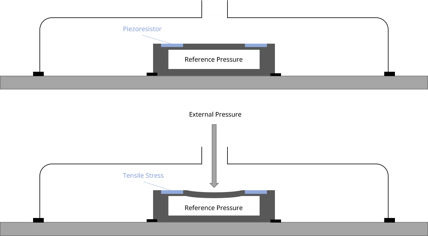
Navigating Pressure Sensor Selection: A Comprehensive Guide for PCB Integration
Improving PCB Reliability through Better Footprints
STM32 Buzzer Music Playback Example
The Ultimate Guide to Component Footprint Library Management: Staying Organized and Efficient
Component Footprints for SMT Assembly: Optimizing for Pick and Place Machines

SMD vs. Through Hole: Optimizing Footprint Design for Different Component Types
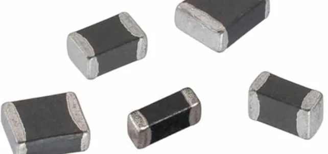
Optimizing SMD Inductor Layouts: A Guide to Enhancing PCB Performance
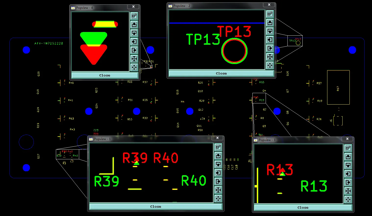
Common KiCad PCB Manufacturing Problems and How to Fix Them