 07:09
07:09
Double-Sided PCB
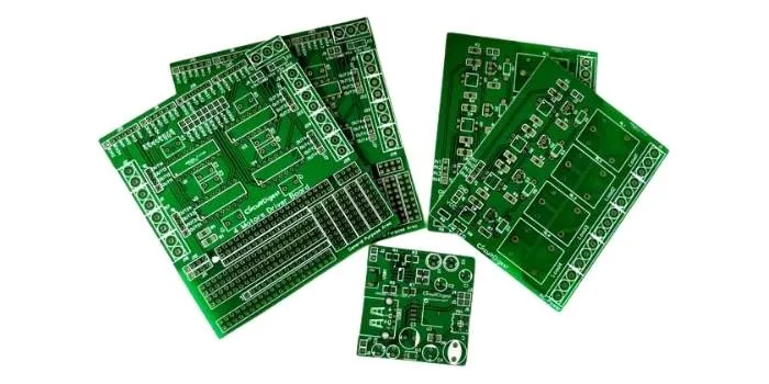
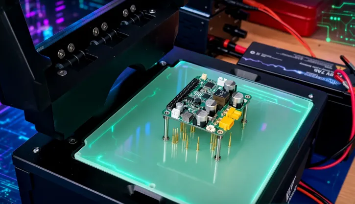
Double-sided PCBs represent a fundamental advancement in printed circuit board technology, featuring conductive layers on both the top and bottom surfaces. This design allows for greater component density and more intricate routing compared to single-sided boards, making them ideal for compact electronic devices where space is at a premium. Engineers and hobbyists often turn to double-sided PCBs for projects requiring enhanced functionality without increasing the board's footprint, such as in audio equipment, power supplies, and sensor modules. By utilizing vias to connect traces between layers, these boards support efficient signal paths and improved thermal management, which are crucial for reliable performance in real-world applications. For those searching for information on double-sided PCBs, this tag compiles a range of articles that delve into design principles, fabrication techniques, and troubleshooting tips. Understanding the layout process is key; for instance, prioritizing ground planes on one side can minimize electromagnetic interference, while careful via placement ensures signal integrity. Practical best practices include selecting appropriate substrate materials like FR-4 for durability and using software tools such as Eagle or KiCad to simulate designs before prototyping. These insights help users avoid common pitfalls, like misalignment during soldering or inadequate trace widths that could lead to overheating. Whether you are prototyping a custom gadget or optimizing an existing circuit, the resources here offer step-by-step guidance on assembly methods, including through-hole and surface-mount technologies. Articles also cover cost-effective manufacturing options, from DIY etching to professional services, empowering you to make informed decisions based on project scale and budget. By exploring these topics, you can gain the knowledge needed to implement double-sided PCBs effectively in your electronics endeavors, fostering innovation and efficiency in your designs.
Video Guide
-
07:09
-
 12:09
12:09
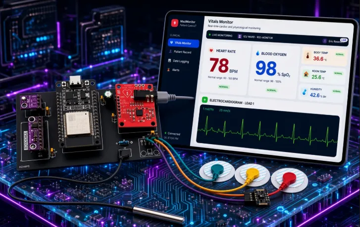
ESP32 Health Monitor PCB: 2-Layer FR-4 DFM for Clean ECG
-
 10:21
10:21
ESP32 Fingerprint Voting Machine Video: Custom 2-Layer PCB Delivers Reliable Biometrics
-
 10:07
10:07
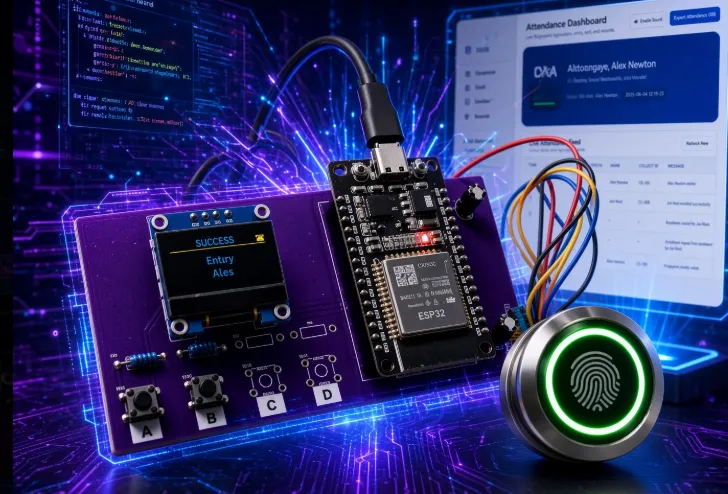
ESP32 Fingerprint Attendance PCB: Reliable 2-Layer Design Ends Breadboard Failures
-
 10:53
10:53
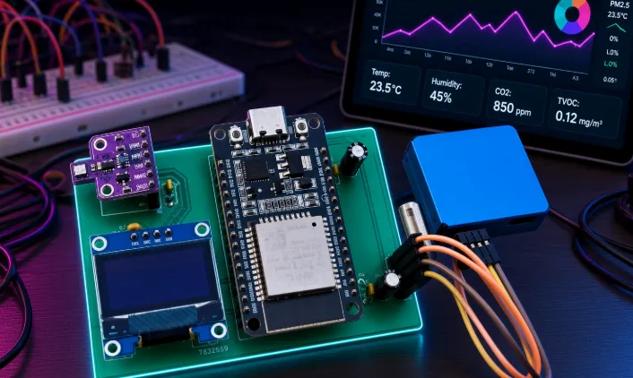
ESP32 Air Monitor PCB: Reliable Custom Board for Clean Sensor Data
-
 00:52
00:52
How Many PCB Layers Do Beginners Actually Need?
Technical Articles
Signal Layers for Beginners: A Hobbyist's Introduction
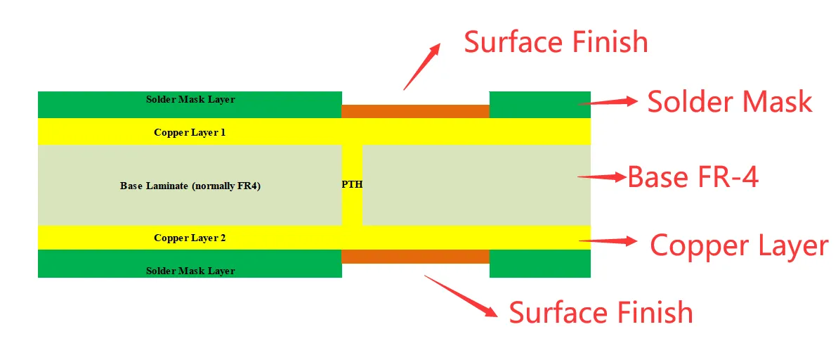
Troubleshooting Common Issues in Double Layer PCBs: A Practical Guide
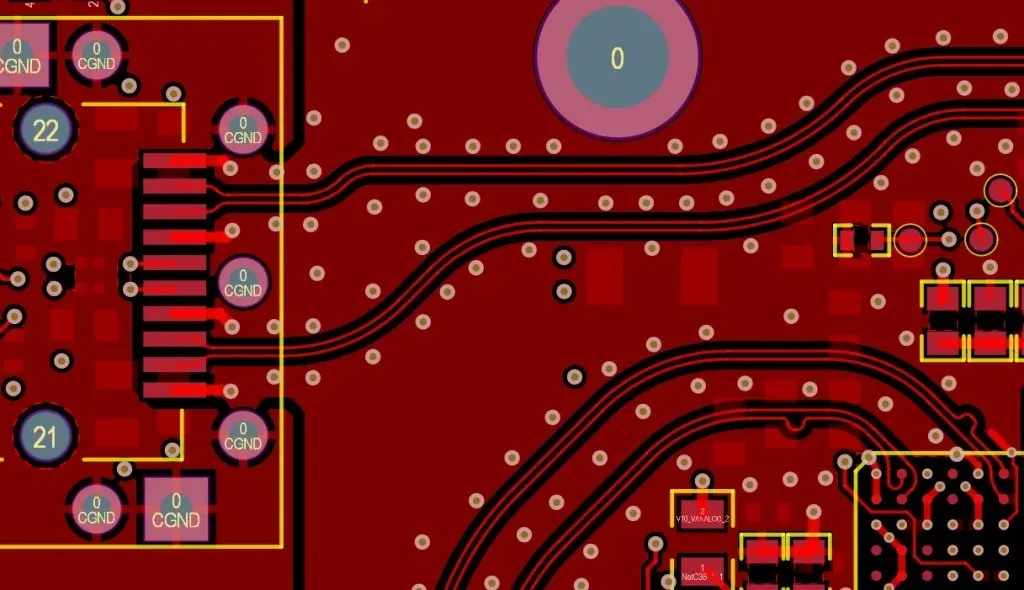
Via Strategies for High Density Double Layer PCBs: Types and Placement
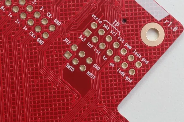
Unveiling the Mystery: When to Choose Non Plated Through Holes for PCB Design
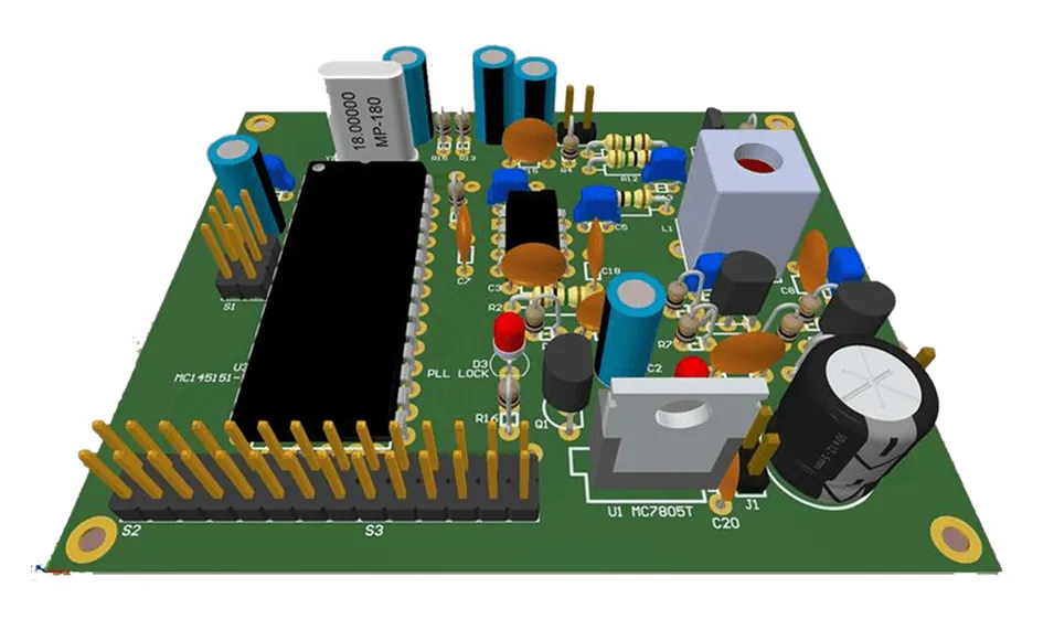
Designing and Assembling PCBs for Robotics Projects: A Practical Guide
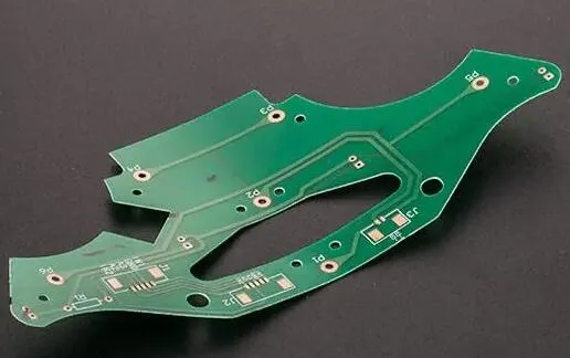
FR-4 PCB Design Fundamentals: A Beginner's Step-by-Step Guide

ESP32 Patient Health Monitor on a 2-Layer PCB: Analog Paths, Headers and DFM

ESP32 Fingerprint Voting Machine: The Custom Double-sided PCB That Changed Everything
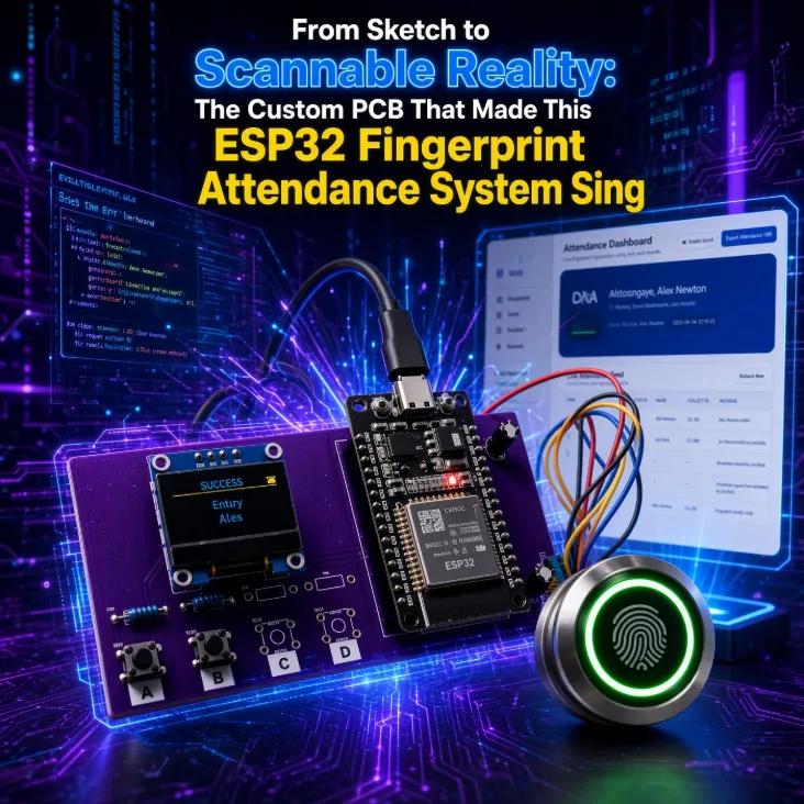
From Sketch to Scannable Reality: The Custom 2-layer PCB That Made This ESP32 Fingerprint Attendance System Sing
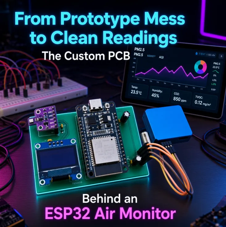
From Prototype Mess to Clean Readings: The Custom PCB Behind an ESP32 Air Monitor
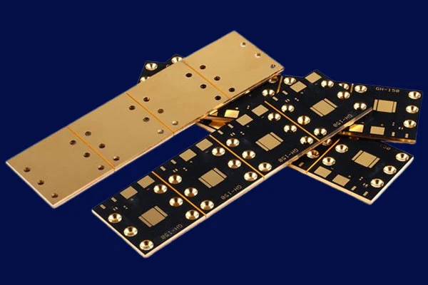
Metal Core PCBs: Enhancing Heat Dissipation with Double Sided Designs
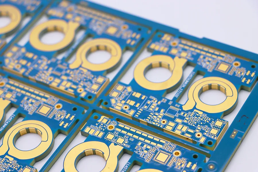
Heavy Copper PCBs: Advantages of Using Double-Sided Designs
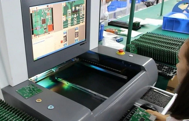
Quality Control and Testing Procedures for Double-Sided PCBs
Common Engineering Queries in 2 Layer FR4 PCB Design and Manufacturing