 03:34
PCB Lamination
A collection of posts on PCB Lamination
Video Guide

Technical Articles
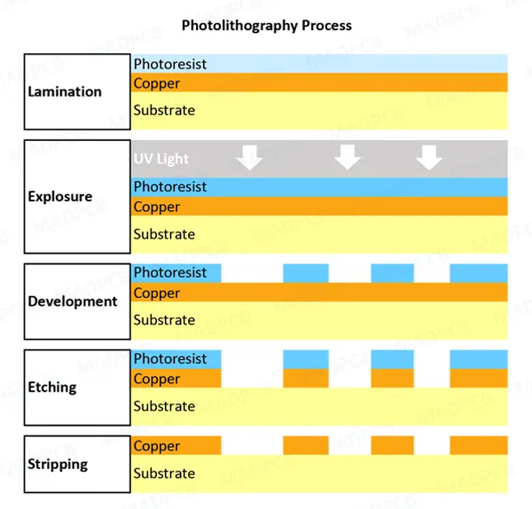
PCB Direct Imaging: Overcoming Challenges with Warped or Uneven Substrates
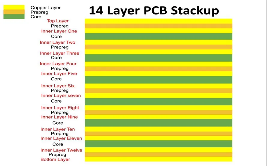
Sequential Lamination for RF and Microwave PCBs: Optimizing Performance in High Frequency Applications
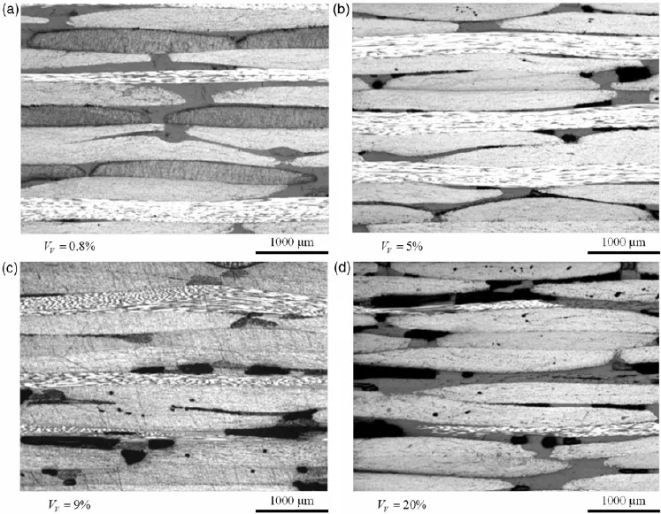
Void Formation in PCB Lamination: Understanding the Mechanisms and Mitigation Strategies
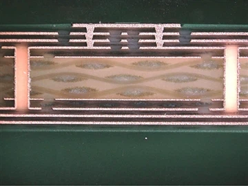
Delamination in PCB Lamination: Causes, Detection, and Prevention
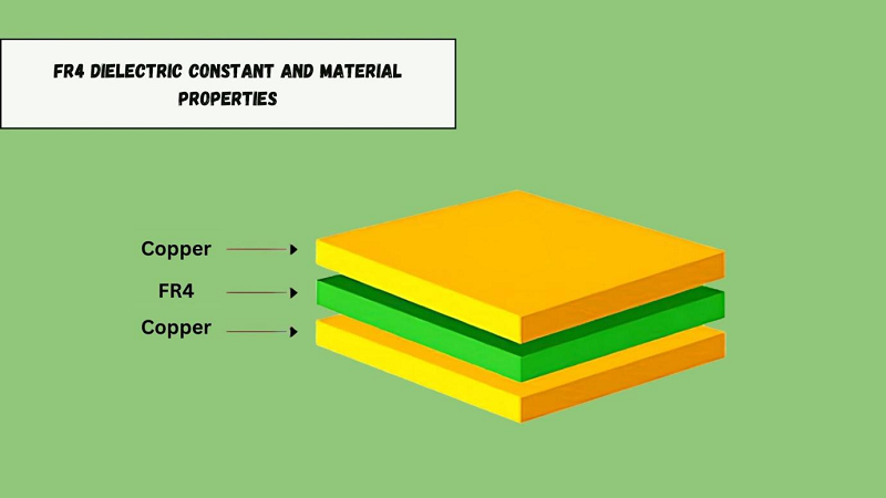
Demystifying FR 4 Manufacturing: A Step by Step Guide
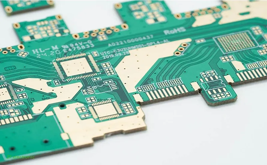
Manufacturing High Tg PCBs: Overcoming Lamination and Soldering Hurdles
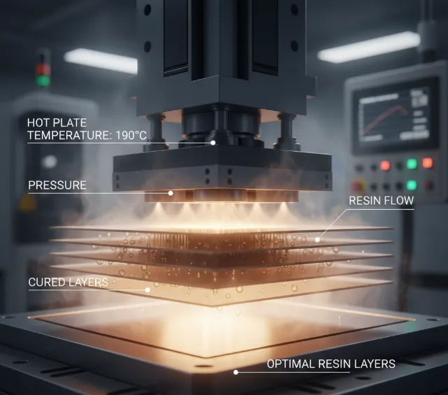
PCB Lamination Temperature Control: A Guide to Process Optimization
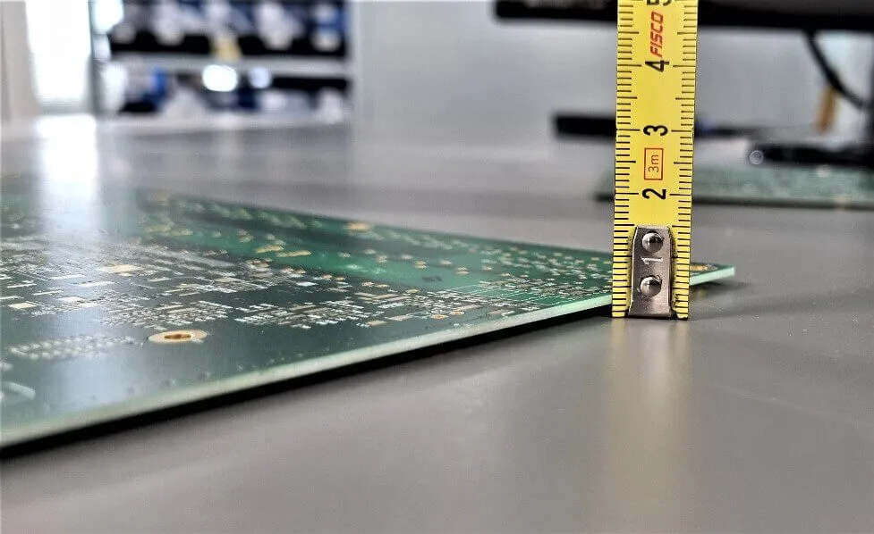
Minimizing Warpage in Multilayer PCB Manufacturing: Causes and Cures
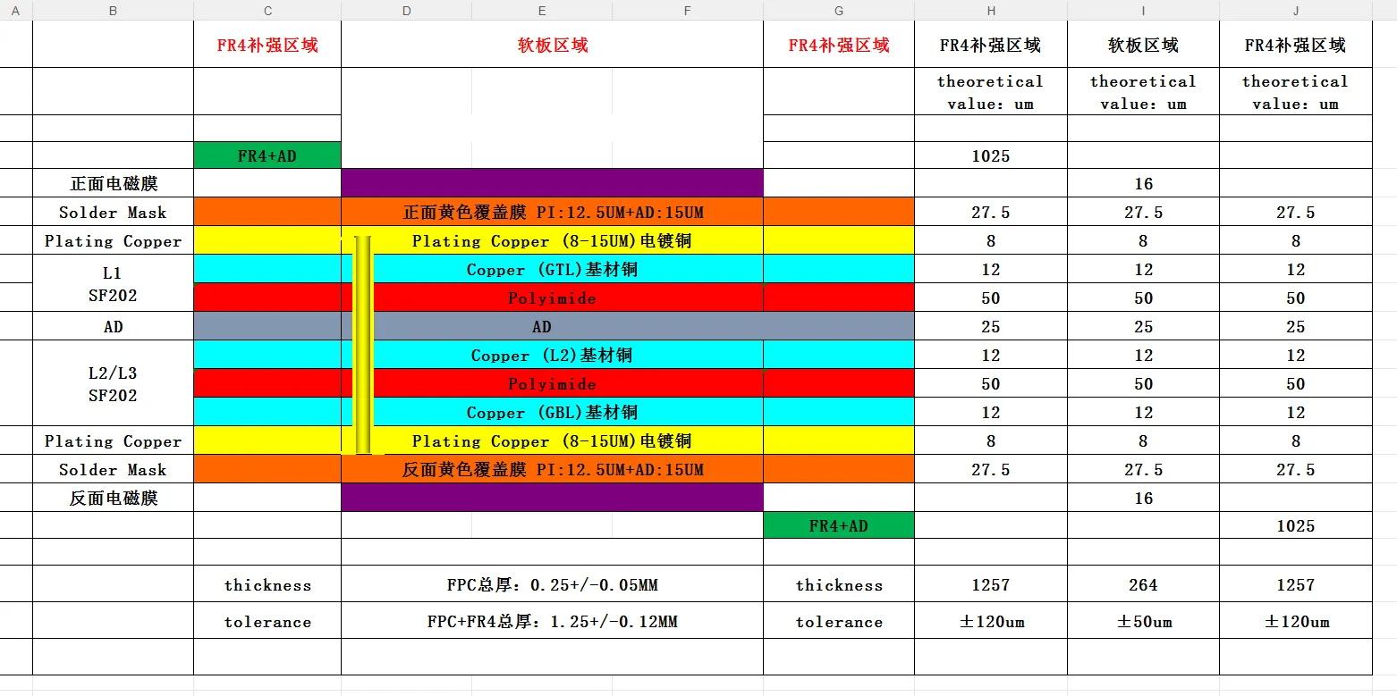
PCB Stackup, Impedance and Thickness Issues in CAM Review
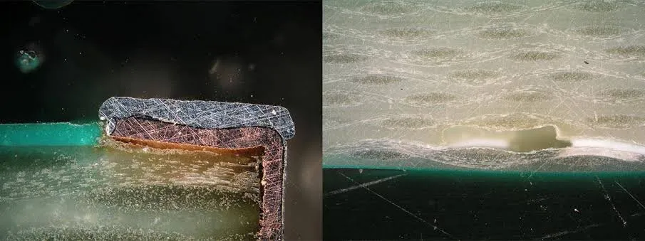
FR4 PCB Resin Void: Causes and Manufacturing Prevention
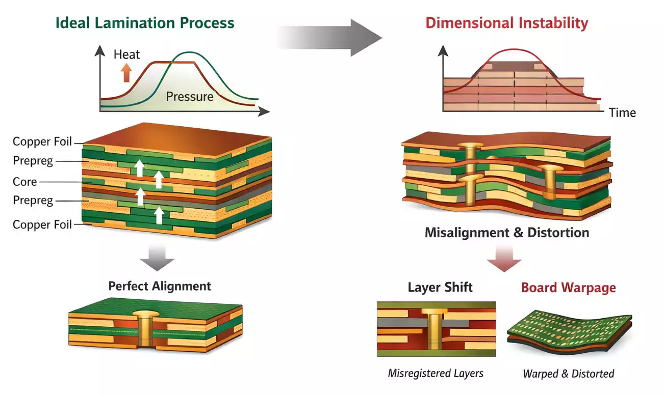
FR4 PCB Registration Accuracy: Causes of Layer Misalignment
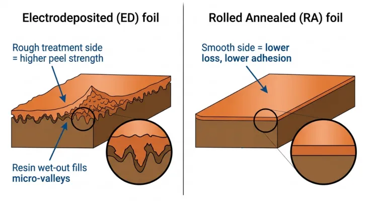
FR4 PCB Copper Foil Peeling: Causes and Prevention
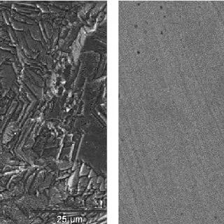
FR4 PCB Surface Preparation Before Lamination
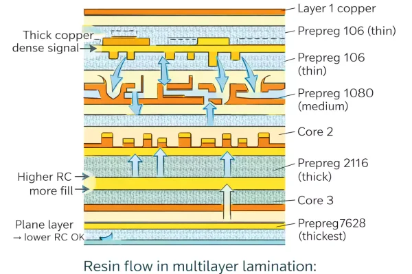
FR4 PCB Resin Flow: Effects on Multilayer Manufacturing
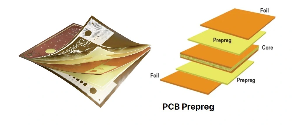
FR4 PCB Prepreg Selection: Resin Content and Thickness Considerations
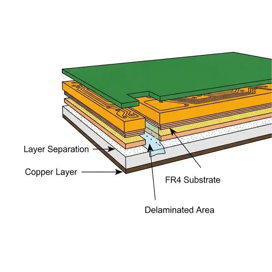
FR4 PCB Delamination: Causes, Detection, and Prevention
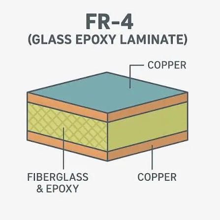
FR4 PCB Inner Layer Oxide Treatment: Purpose and Process Control
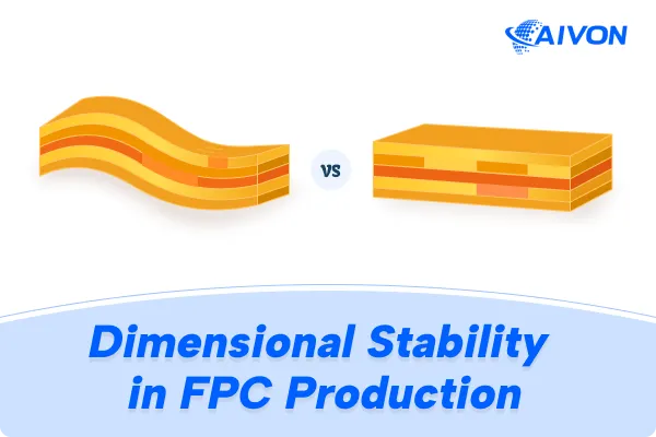
Dimensional Stability in FPC Manufacturing: Causes and Solutions
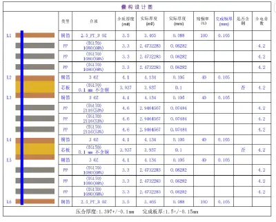
How a 0.1 mm Stackup Mismatch and Material Shortage Halted a 6-Layer 3 oz PCB Order