02:50
02:50
Solder Mask
Solder mask is a crucial protective layer applied to printed circuit boards (PCBs) during manufacturing, serving as a barrier against oxidation, solder bridging, and environmental contaminants. This thin polymer coating, often green but available in various colors, covers the copper traces while leaving pads and vias exposed for soldering. For engineers, hobbyists, and manufacturers searching for information on solder mask, this tag compiles essential resources that explain its role in enhancing PCB durability and reliability. Understanding solder mask properties can help prevent common issues like short circuits and improve overall board performance in high-stakes applications such as consumer electronics, automotive systems, and medical devices. In practical terms, selecting the right solder mask involves considering factors like thermal resistance, adhesion strength, and compatibility with assembly processes. For instance, liquid photoimageable (LPI) solder masks offer precise application for fine-pitch components, while dry film options provide robust protection in harsh environments. Best practices include ensuring proper curing temperatures to avoid defects and conducting thorough inspections to verify coverage uniformity. These insights are particularly valuable for those troubleshooting PCB failures or optimizing designs for mass production, where solder mask can significantly reduce rework costs and extend product lifespan. The articles linked under this solder mask tag offer detailed guides on application techniques, material comparisons, and troubleshooting tips, drawing from real-world case studies and industry standards. Whether you are designing your first prototype or refining advanced multilayer boards, these resources provide the knowledge needed to make informed decisions and achieve professional-grade results.
Video Guide
-
02:50
-
 03:41
03:41
PCB Solder Mask Bridges Issues: Fine-Pitch DFM
-
 00:51
00:51
PCB Vias Plugging: Manufacturing Process, Failure Modes, and Reliability Impact
-
 00:57
00:57
PCB Solder Mask: Essential Protective Layer in Manufacturing
-
 01:00
01:00
Solder Mask Bridge in PCB Manufacturing: Preventing Shorts in Fine-Pitch Designs
-
 03:32
03:32
Solder Mask Application Process in PCB Manufacturing: Factory Tour and Critical Controls
-
 07:01
07:01
Inside the Modern PCB Factory: From Design to High-Volume Production
Technical Articles

Solder Mask vs. Paste Mask: Why a 0.1 mm Error Can Scrap an Entire PCB Batch
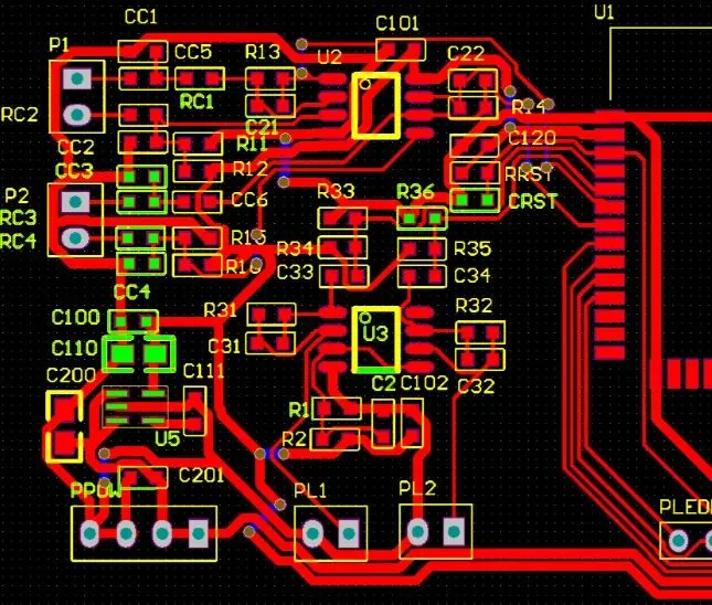
Should PCB Silkscreen Printing or ENIG Surface Finish Come First After Solder Mask?

CAM Confirmation of Fiducial Marks on a 205 × 20 mm 6-Layer Rigid-Flex Panel

Root Cause Analysis and Control of the Galvanic Effect in PCB Immersion Silver

What Manufacturing Teaches Design: Lessons from a Soldering Quality Problem

Causes and Prevention of Solder Balls in Wave and Selective Soldering

Solder Mask vs. Paste Mask: Essential Differences for PCB Design
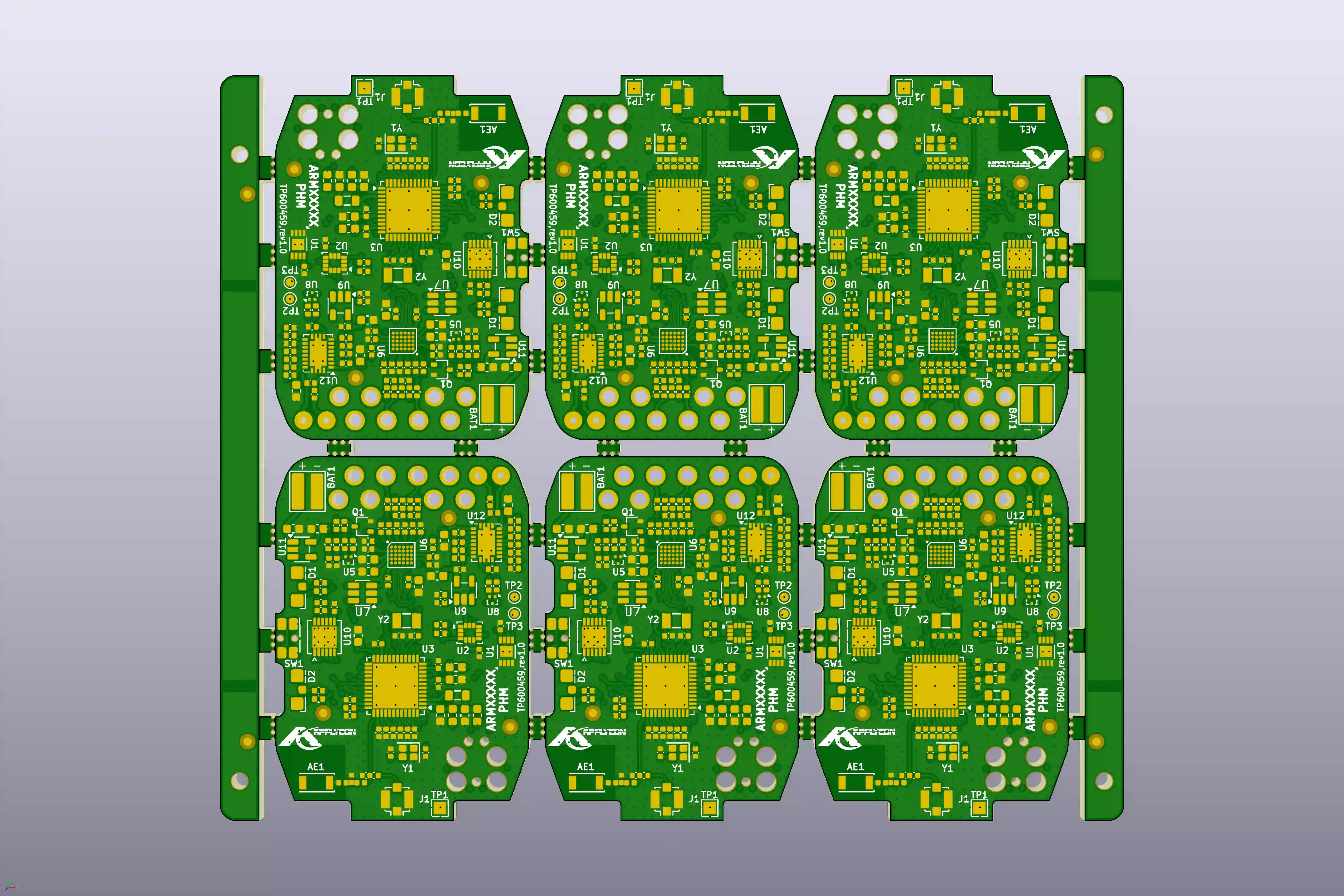
How to Avoid Common Solder Mask & Stackup Issues in 6-Layer HDI PCBs
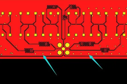
How to Fix CAM Issues in 4-Layer Rigid-Flex PCB Designs

8-Layer FR-4 PCB with Blind Vias: Solder Mask Openings, Via Plugging and V-CUT Clearance Issues During CAM Review
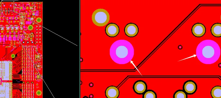
14 Layer TG170 PCB Manufacturing Review for Impedance and Resin Plugging
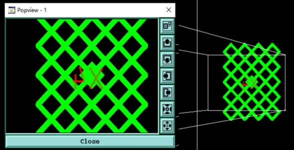
How We Fixed Solder Mask Bridges, Copper Density & Via Issues in Thin 6-Layer HDI PCB
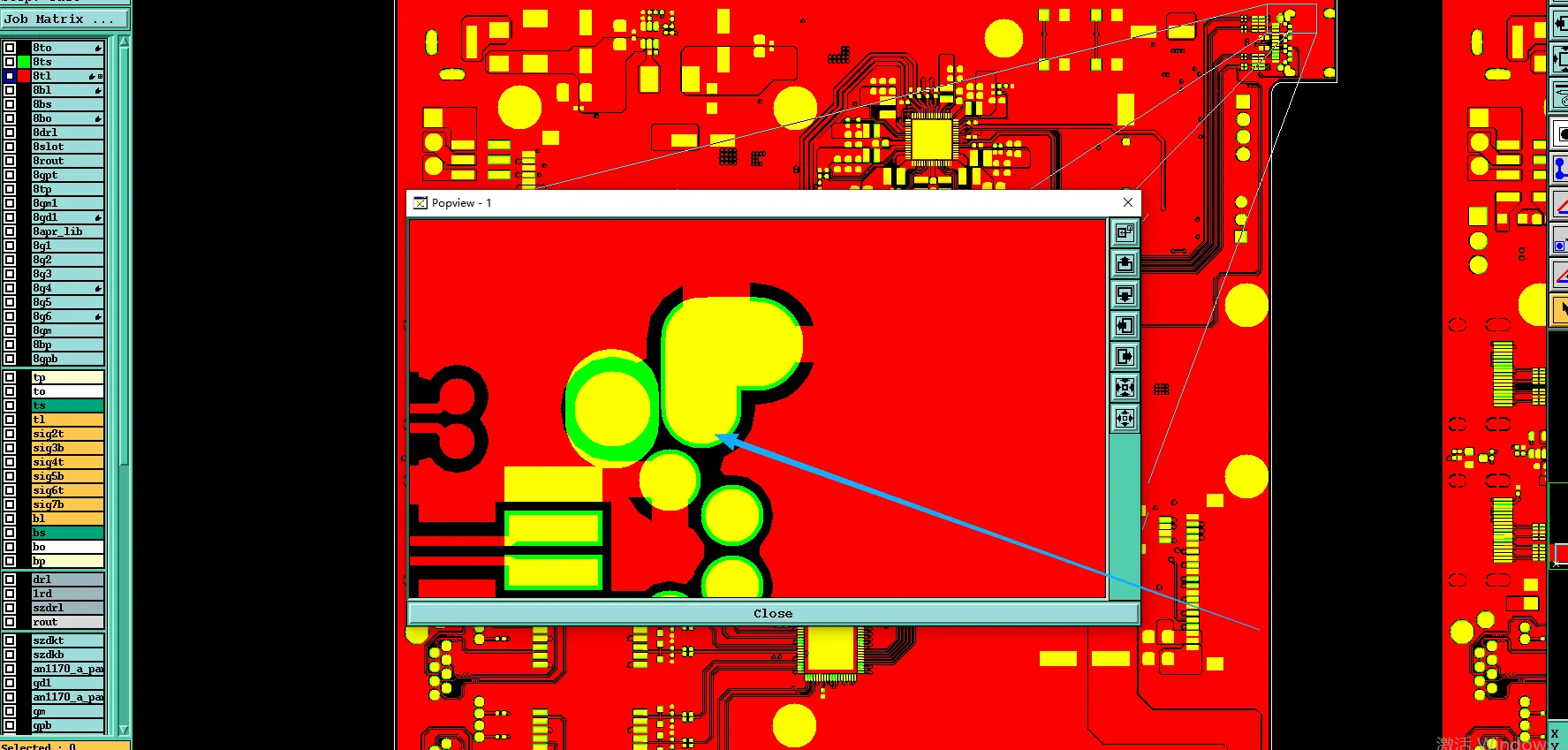
How to Fix Tight Pad Spacing and Impedance EQs in 8-Layer PCB CAM Review
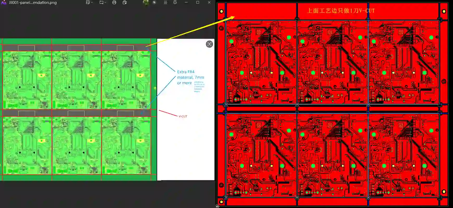
How to Solve 2-Layer PCB CAM Issues Before Manufacturing
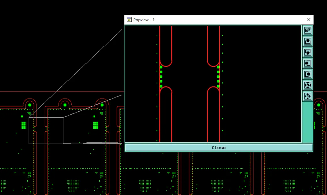
How to Prevent Solder Mask Bridge Failure and NSMD BGA Issues in 8-Layer PCB
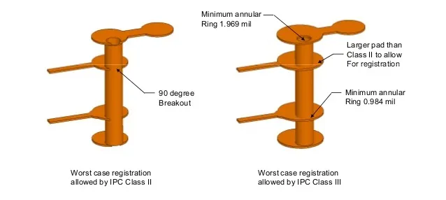
5 Critical PCB Manufacturability Checks You Can't Afford to Skip
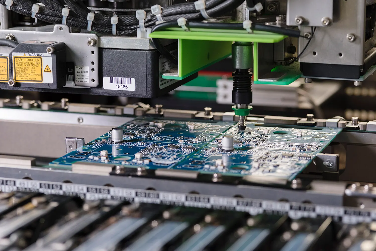
Design for Assembly Checklist: 10 Steps to Streamline Your PCB Assembly Process
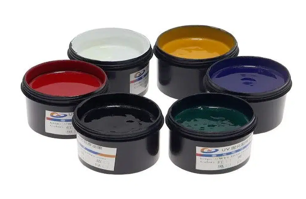
DIY Solder Mask Application: A Simple Guide for Electronics Enthusiasts
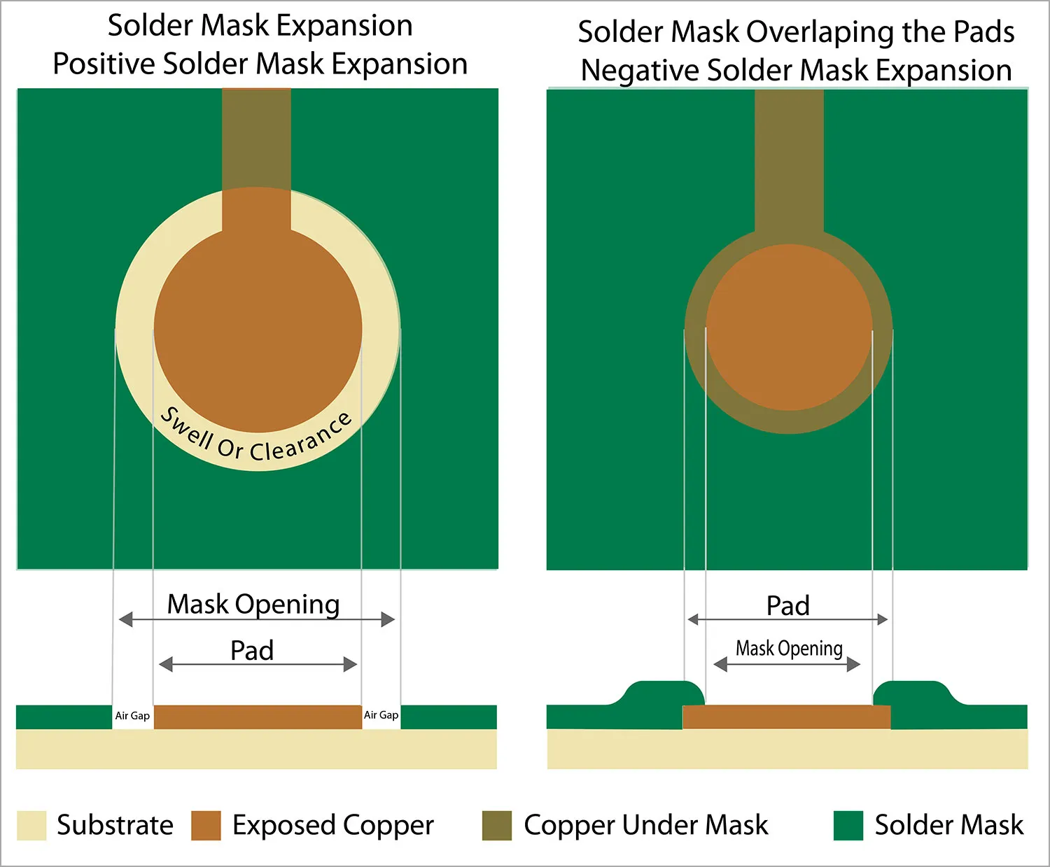
Understanding Solder Mask Expansion: Best Practices for Reliable PCB Assembly