 00:52
00:52
Via Stitching
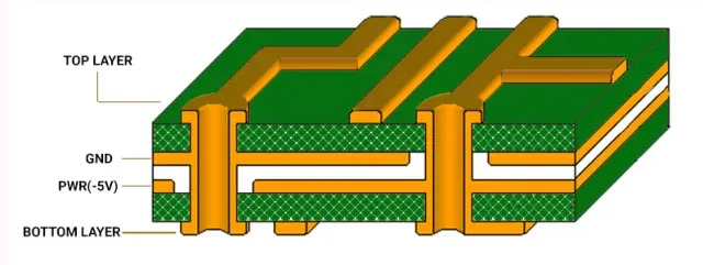
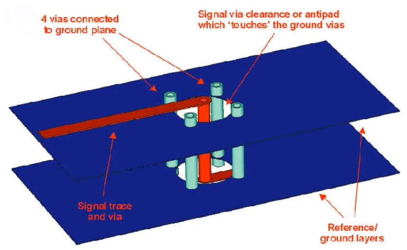
Via stitching is a critical technique in printed circuit board (PCB) design that involves placing multiple vias in a patterned arrangement to connect layers, typically for grounding, shielding, or thermal dissipation purposes. This method enhances the electrical performance of PCBs by reducing impedance, minimizing electromagnetic interference (EMI), and improving signal integrity in high-speed or high-frequency applications. For engineers and designers searching for via stitching, understanding its implementation can significantly optimize board layouts, especially in multilayer designs where maintaining a low-inductance path is essential for reliable operation. In practice, via stitching is often applied around sensitive components or along the edges of ground planes to create a Faraday cage-like effect, effectively containing noise and preventing crosstalk. Best practices include spacing vias at intervals no greater than one-eighth of the wavelength of the highest operating frequency to ensure effective shielding. Additionally, thermal via stitching under power components helps dissipate heat more efficiently, extending the lifespan of the board and its elements. Designers should consider factors such as via diameter, pitch, and fill type—whether tented, plugged, or filled—to balance manufacturability with performance needs. Tools like Altium Designer or KiCad offer features to automate via stitching patterns, allowing for precise control and simulation before fabrication. For those delving deeper into PCB optimization, the articles linked under this tag provide detailed case studies, tutorials, and comparisons with alternative techniques like via fencing. By applying these insights, you can refine your designs to meet stringent industry standards, from consumer electronics to aerospace systems, ensuring robustness and efficiency in your projects.
Video Guide
-
00:52
Technical Articles

Should You Use Solid or Hatched Copper Pour on PCBs?

Why Do Eye Diagrams Collapse Even When High-Speed Interface Traces Are Length-Matched?

Adding Via Stitching in KiCad with the kicad-action-scripts Plugin
Altium Designer Q&A: Import/Export Rules, Single-Sided PCB Setup, Via Stitching, and Practical Workflow Tips
Ground in Electronic Circuits: Signal Ground, Power Ground, Ground Partitioning, Guard Ground, and Single-Point Grounding
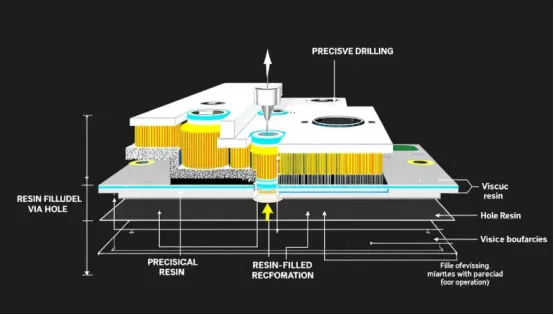
Which Vias Need Resin Plugging? Real Engineer Questions from Production
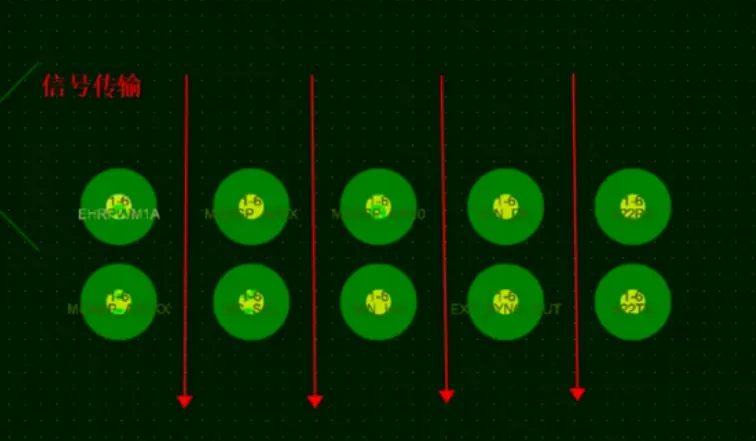
High-Speed PCB Vias: A Small Feature That Can Break the Signal
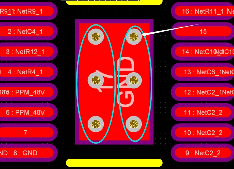
Why More Thermal Vias Do Not Always Mean a Lower PCB Temperature
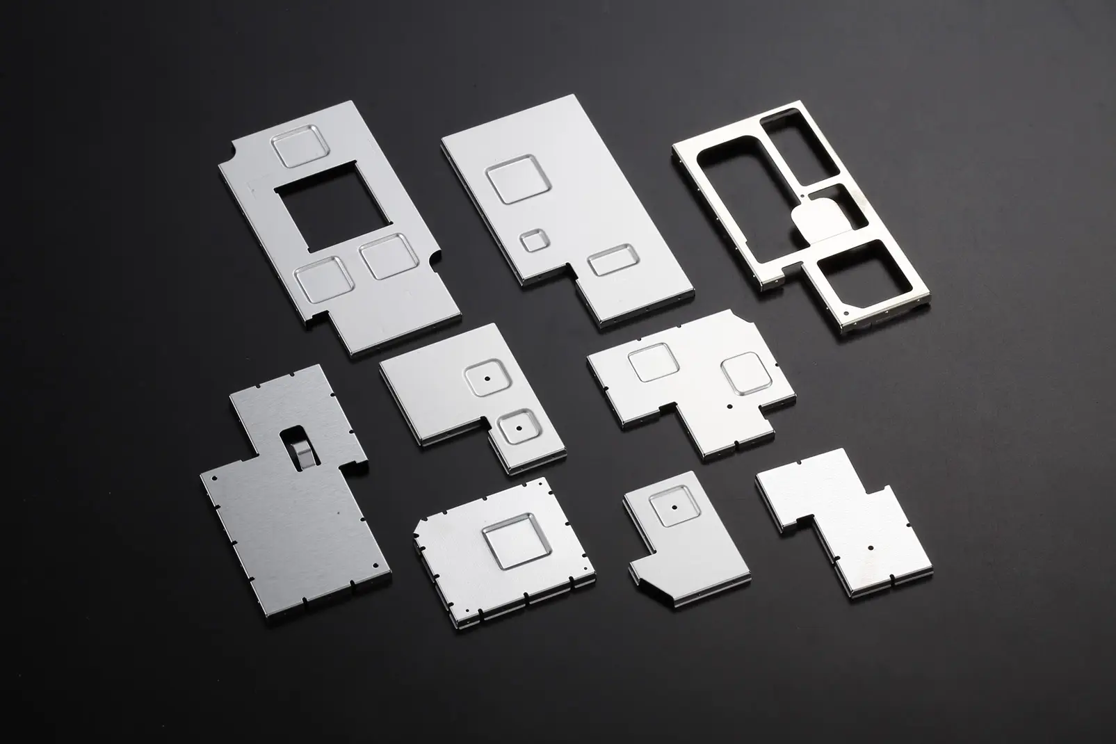
Optimizing EMI Shielding in Consumer Electronics for Regulatory Compliance

Beyond the Basics: Advanced Automotive PCB Design Techniques
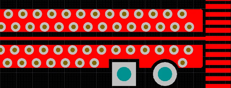
Ground Plane Stitching: Achieving Optimal Grounding in Multi Layer PCBs
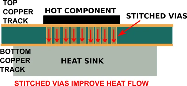
Thermal Via Stitching: Cooling Your High Power PCBs
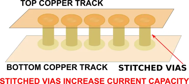
Via Stitching: Your Secret Weapon for Reducing EMI in PCBs
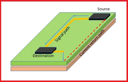
Through Hole Via Placement Strategies for Optimal Signal Routing
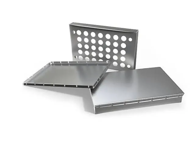
EMI Shielding Design Guide for Sheet Metal Enclosures
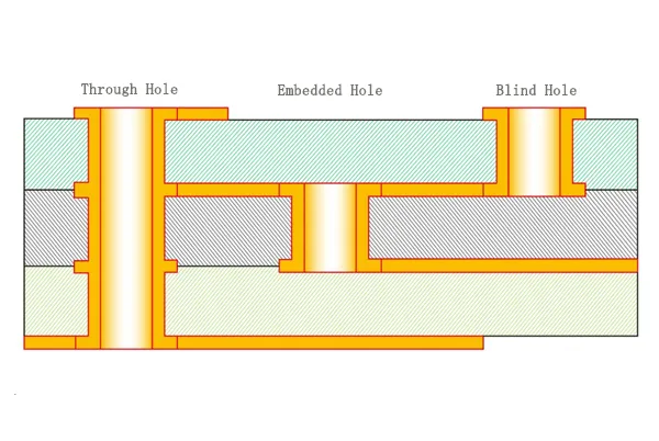
Optimizing Via Design in Rigid Flex PCBs: Enhancing Electrical and Mechanical Performance
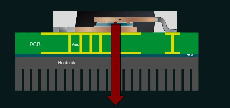
Thermal vias: how to use it properly and improve cooling performance.
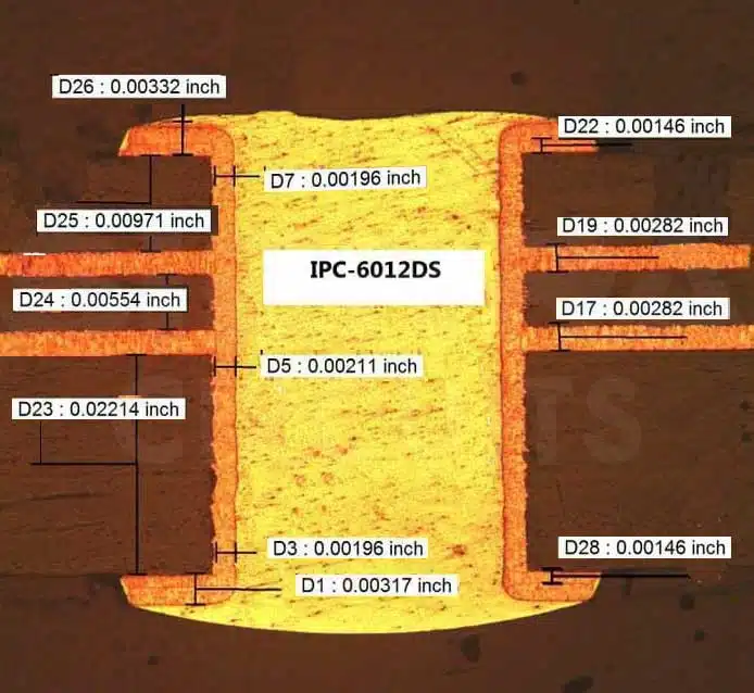
Minimum Drill Size for High Current PCBs: Thermal Management Strategies
Via Stitching: A Comprehensive Guide to Enhancing Grounding and Shielding in PCBs