










Engineering Cases
Engineering Cases focuses on real PCB engineering reviews, manufacturing challenges, and production optimization processes from actual fabrication projects. This category highlights how different PCB designs are evaluated and adjusted during engineering review, covering topics such as stack-up analysis, impedance control, drill optimization, copper balancing, solder mask alignment, DFM review, and production risk assessment across various PCB applications. The content in this section is based on practical manufacturing scenarios rather than theoretical introductions. Each engineering case demonstrates how specific PCB issues are identified, analyzed, and resolved during production preparation and fabrication. These records help engineers, purchasers, and hardware teams better understand the relationship between PCB design decisions and manufacturing stability, yield control, and process reliability. Topics may include multilayer PCB engineering review, HDI process optimization, flexible PCB manufacturing considerations, heavy copper processing adjustments, surface finish selection, Gerber data verification, and other real-world PCB production experiences. By organizing engineering challenges and process solutions into structured case content, this category provides valuable insight into practical PCB manufacturing and engineering workflow management.
Featured Blog
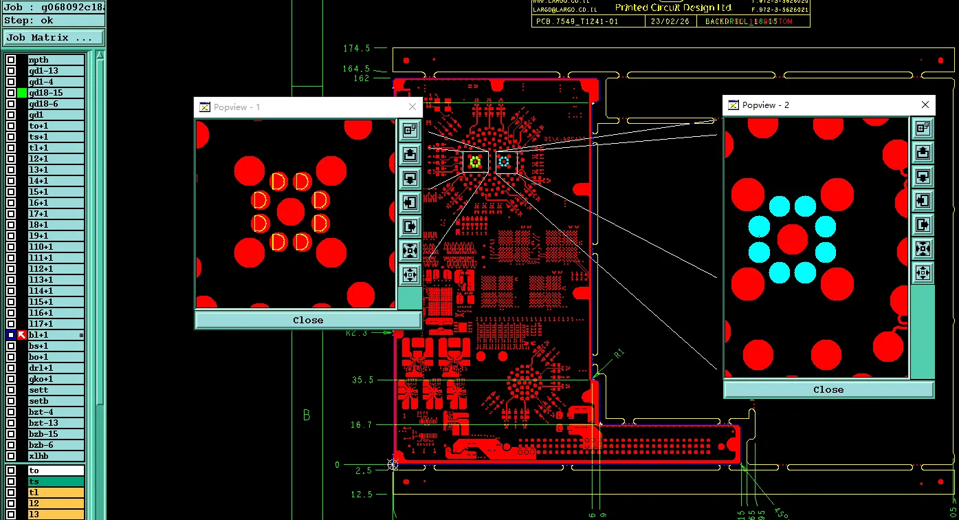
PCB Hole Attributes and Special Drilling: Common CAM Review Conflicts
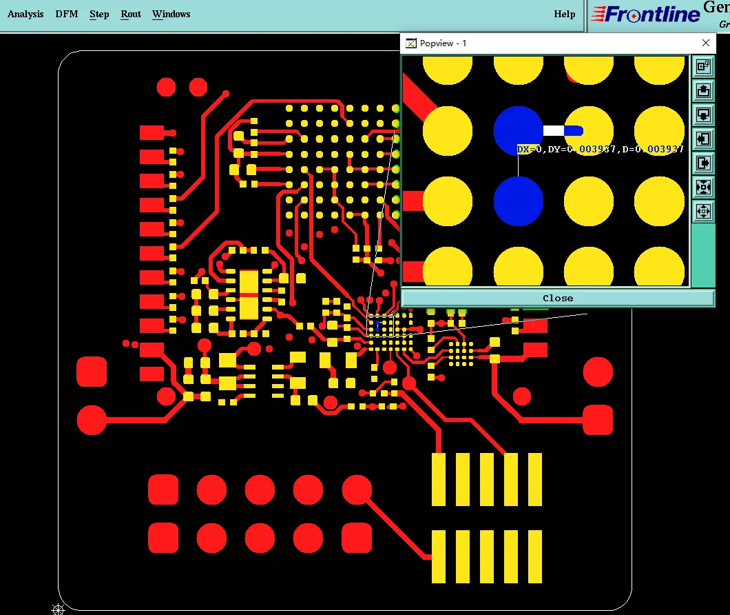
See how CAM reads PCB hole attributes and special drilling—PTH vs NPTH, back drill, press-fit holes, countersink, and laser vias—and why incomplete data delays fabrication.
Latest Blogs

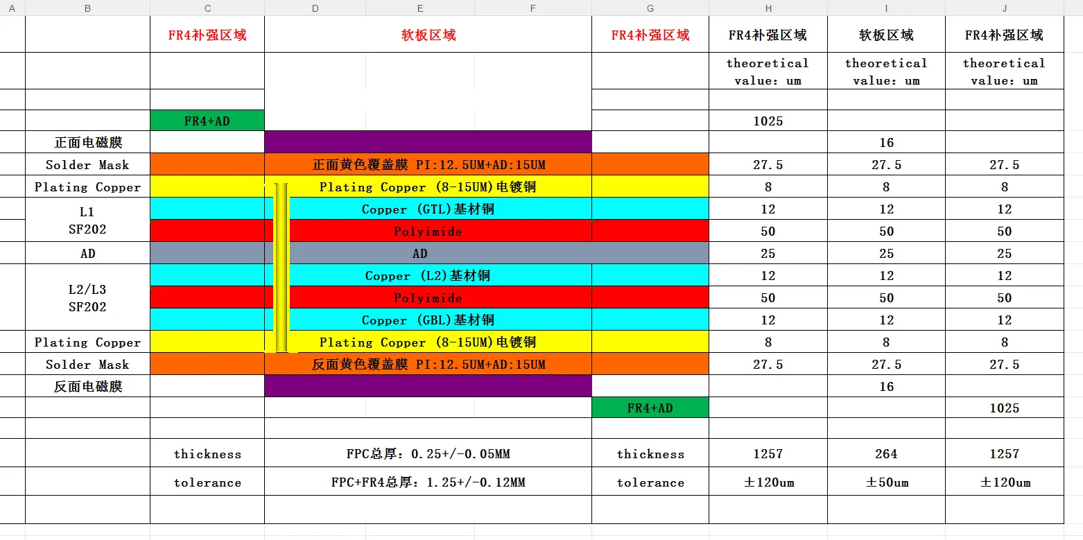
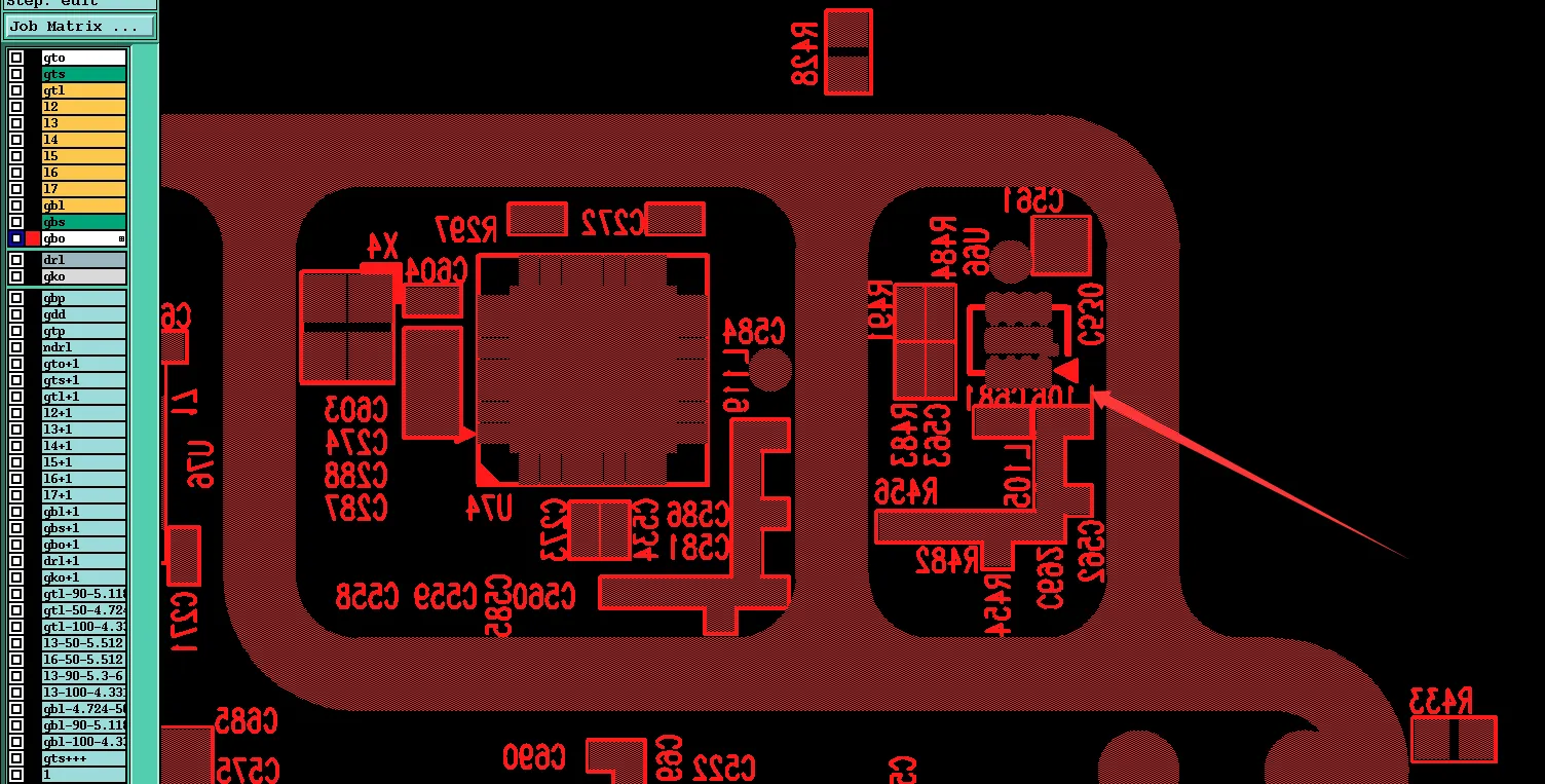
When Bottom Silkscreen and PI Stiffener Specs Conflicted on a 0.2 mm 4-Layer Flexible PCB
CAM review of a 0.2 mm 4-layer flexible PCB revealed non-mirrored bottom silkscreen and conflicting PI stiffener thickness between contract (0.3 mm total) and Gerber data. Customer confirmation was required before production release.

Optimizing PCB Panelization for 8-Layer Production
Learn how CAM engineers optimized process rails and panelization for an 8-layer 0.8 mm PCB, adjusting to a 113.5 × 118 mm 5×3 panel to create a production-ready manufacturing package and improve fabrication efficiency.

Why Identical Drill and Pad Sizes Risked Via Failures in a 6-Layer FR4 PCB
A DFM review of a high-density 6-layer FR4 PCB caught identical drill and pad sizes with no copper connection, risking weak or missing via plating. Clarifying hole attributes as NPTH, documenting missing positioning holes, and fixing silkscreen overlap prevented opens, registration errors, and yield loss before production.

Missing Single Outline, Edge Copper, and Unopened SMD Pads on a 4-Layer HDI Order
CAM review of a 4-layer HDI board with customer self-panelization uncovered a missing single outline, copper too close to edges, holes matching pads, and SMD pads lacking solder mask openings. Proposed clearances and fixes required confirmation.

PCB Hole and Slot Tolerance Conflicts: CAM Cases from Production
When PCB hole tolerance or slot size is too tight to drill, CAM compares the hole chart with Gerber. Confirm the released band, accept routing and ±0.1 mm on named tools, or revise plated and NPTH calls.

How PCB CAM Resolves Blind Via Size and Edge Clearance Issues
CAM review of blind and buried vias checks released size on HDI pairs against laser drilling, and via-to-edge clearance to the outline. Confirm keep, shrink, or relocate before build.

PCB CAM Case Study on Tight Tolerances in Backdrilling, Countersink, and Press-Fit Holes
How PCB CAM reviews a tight backdrill stub, countersink depth versus finished board thickness, and press-fit hole tolerance on large tools—what the files show and what must be confirmed.
Why PCB CAM Must Verify PTH and NPTH Hole Definitions
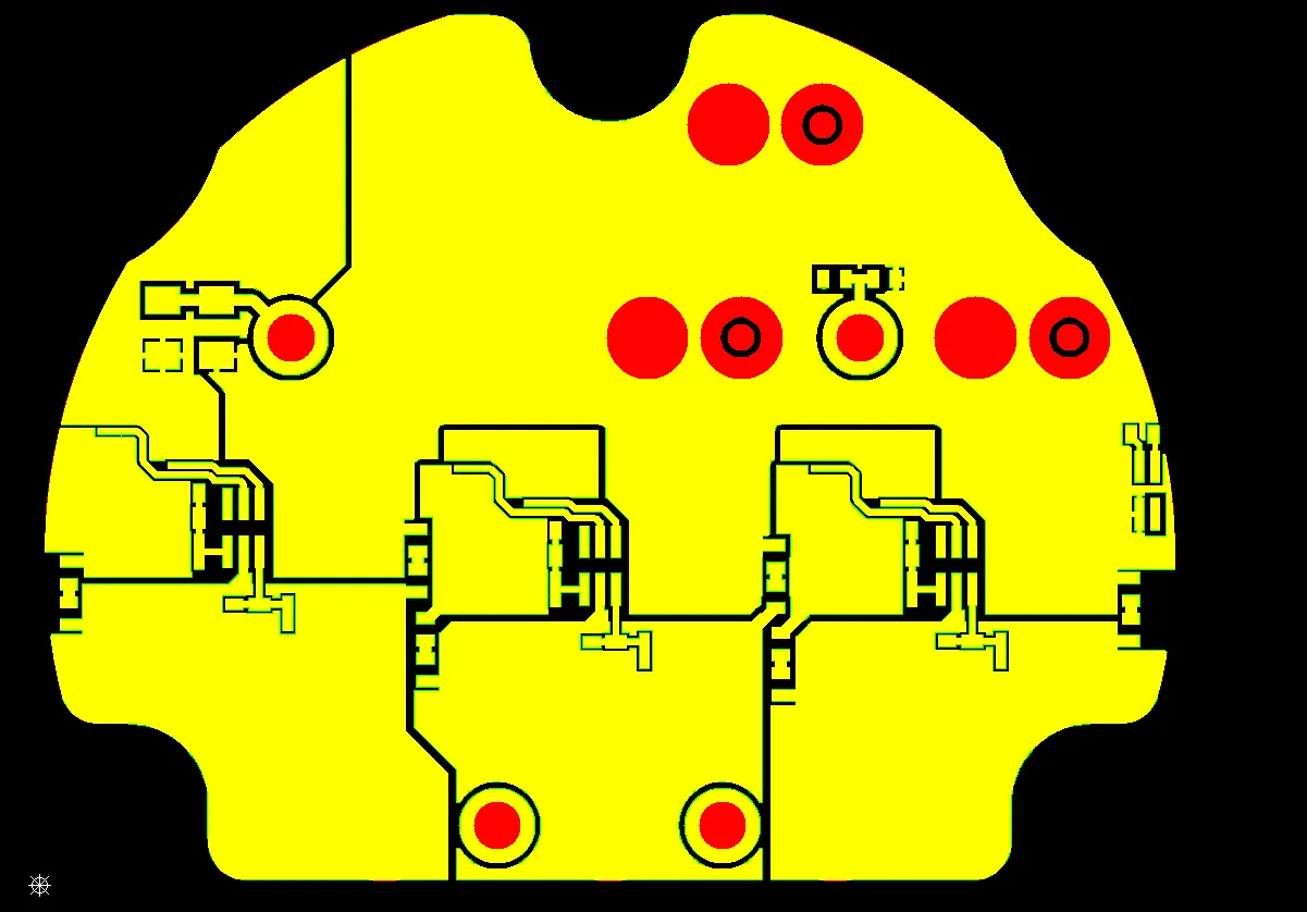
PTH vs NPTH conflicts appear when the hole chart and Gerber through-hole pads do not match. This CAM review covers plated vs non plated through holes, pad-to-drill overlay, and what to confirm before hole plating.

How PCB CAM Balances Copper Thickness, Trace Spacing, and Impedance Requirements
CAM review when PCB copper thickness, copper weight, and finished copper thickness conflict with trace spacing or impedance: 3 oz vs 6.89 mil, two ounce calls, and 0.5 oz base vs 1.5 oz after hole copper.
How PCB CAM Resolves Conflicting Impedance Control Requirements
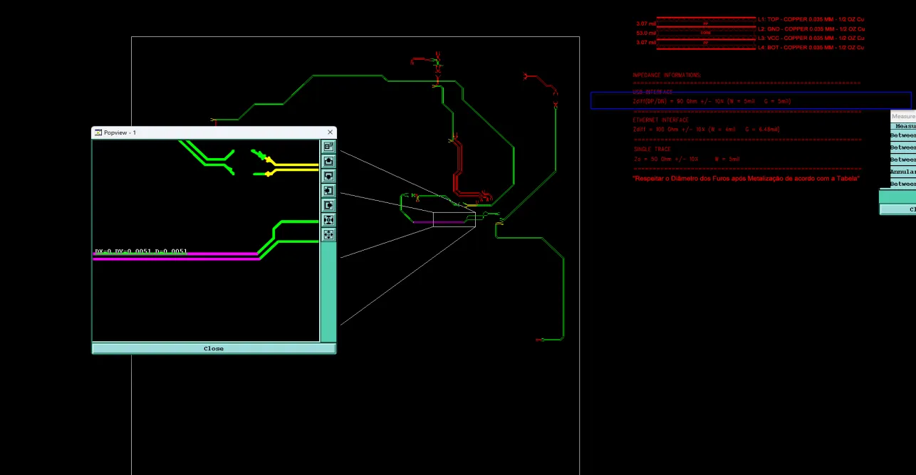
CAM review of PCB impedance control when the table and Gerber conflict—missing 90 ohm 5/5 mil traces, 4.16/7 mil swaps, or one width for 100 ohm differential and 50 ohm. What gets measured and what you confirm.
PCB CAM Review to Overcome Complex Stackup and Lamination Challenges
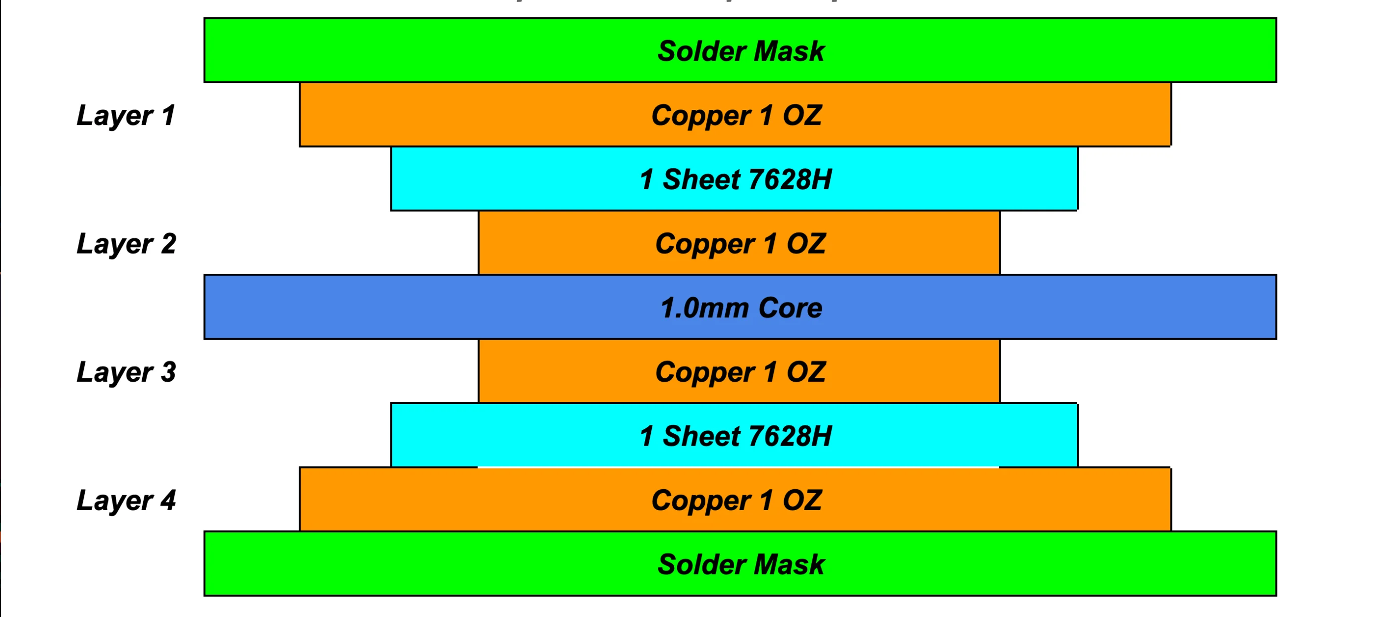
CAM review of PCB stackup and lamination when the drawing and press figure, core and prepreg, copper thickness, and inner-layer copper do not agree. Confirms which construction to press.
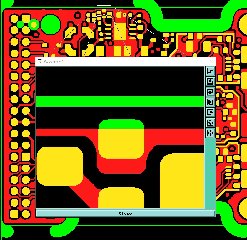
PCB CAM Review for Copper and SMD Pads Near the Board Edge
How CAM reviews PCB edge clearance on the outline overlay. When a copper pour or SMD pad sits on the outline or a V-cut, the close is accept edge copper exposure, confirm a copper shave, or confirm a pad trim.


