


PCB Design
Printed Circuit Board (PCB) design forms the backbone of modern electronics, enabling the creation of compact, efficient, and reliable devices that power everything from smartphones to industrial machinery. In this category, readers gain access to a comprehensive collection of resources dedicated to mastering PCB design principles and techniques. Whether you are a seasoned engineer refining complex layouts or a newcomer learning the fundamentals, these articles provide the knowledge needed to tackle real-world challenges in electronics development. The scope of PCB design covered here extends from initial schematic capture to final board fabrication and testing. Articles delve into essential topics such as layer stacking, signal integrity, thermal management, and component placement strategies. Guides and tutorials offer step-by-step instructions for using popular software tools like Altium Designer and KiCad, while insights explore emerging trends like flexible PCBs and high-speed designs. Best practices emphasize error reduction, cost optimization, and compliance with industry standards, ensuring designs are not only functional but also manufacturable at scale. Real-world applications highlight the category's practical value, demonstrating how effective PCB design contributes to innovations in automotive systems, medical equipment, renewable energy solutions, and consumer gadgets. By addressing common pitfalls and sharing expert tips, these pieces equip professionals to enhance product performance and reliability. Readers benefit from building a deeper understanding through interconnected articles that cover foundational concepts alongside advanced methodologies, fostering continuous improvement in electronics projects. For those involved in prototyping or production, the technical relevance of this content lies in its focus on efficiency and innovation. Detailed discussions on impedance control, EMI shielding, and design for manufacturability prepare you to meet the demands of today's fast-paced tech landscape. Engaging with multiple articles in this category allows for a progressive learning path, where foundational knowledge supports exploration of specialized topics, ultimately leading to more robust and innovative PCB designs.
Featured Blog
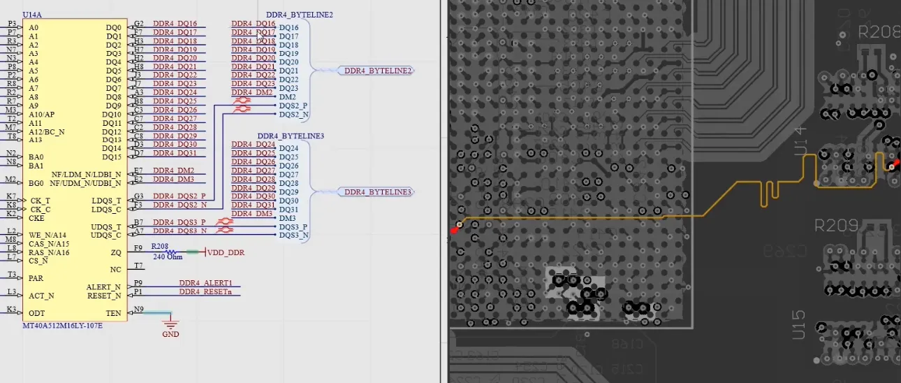
PCB Design Review for Beginners: A Step by Step Guide
Learn how to perform a PCB design review with a practical checklist covering schematics, layout, DRC, manufacturability, and pre-production checks.
Latest Blogs
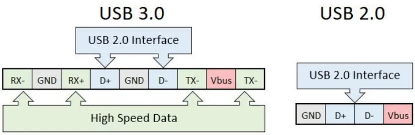
A USB Port Looks Simple. A Bad PCB Layout Turns It Into a Signal Problem
USB 2.0/3.0 and Type-C fail from layout more than from silicon. Hold 90 Ω pairs, short paths, return vias, shell-ground isolation, and treat CC1/CC2 as critical nets.

Repeated EMC Fixes Failed Until This Hidden Noise Source Was Found
An industrial four-layer board failed 200–400 MHz radiated emissions until return ground vias were added at SPI and SRAM layer changes, cutting loop area and the peaks.

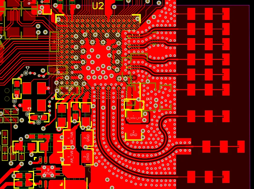
Both Differential Lines Are Length-Matched. Why Is EMI Still Worse?
Equal P/N length does not prove balance. Layer, reference, via, pad, and copper asymmetry convert differential energy to common mode and raise EMI and eye-closure risk.

Denser Vias, More Stable? When a Signal Crosses a "Via Wall," the Reference Plane May Already Be Cut Apart
A DRC-clean via array can still slot the reference plane. When a high-speed trace crosses that via wall, return current detours, impedance shifts, and coupling risk rises.

High-Power PCB Layout: Power Board or Latent Failure?
High-power boards fail on loop area, creepage, temperature rise, and EMI—not missing nets. Cases from a 20 W flyback to 3.5 kW totem-pole PFC + LLC and PV inversion.

Why Does Assembly Still Jam When Clearance Was Left Beside the Connector?
PCB clearance beside a press-fit connector can still fail at assembly. Check the 3D envelope of the housing, shroud, press head, mating path, and stacked tolerances—not pad spacing alone.

Why Add a Midpoint Bias When Converting a Dual-Supply Op-Amp to Single Supply?
Moving an op-amp from dual to single supply leaves no room for the negative half-cycle. Midpoint bias (VBIAS) recenters the AC signal so input and feedback can swing both ways.
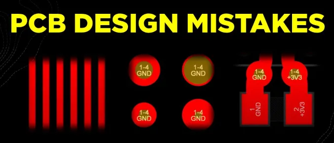
The Ten Most Common Beginner Mistakes in PCB Layout
Default DRC, right-angle traces, distant decoupling, split planes, thin power traces, and missing test points still cause most first-board failures. Check these ten items.
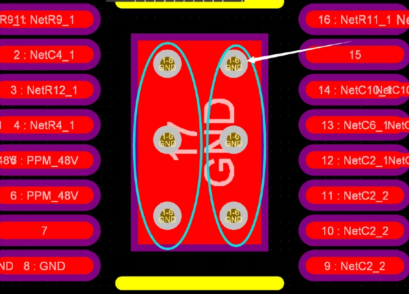
Why More Thermal Vias Do Not Always Mean a Lower PCB Temperature
Via count only opens a local path. Temperature drops when via-wall copper, plane continuity, and the external cooling interface form one low-resistance thermal path.

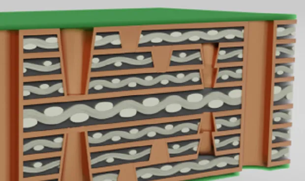
Why Backdrill Stubs Can Still Be Too Long After the Layer Pair Is Correct
A correct backdrill layer pair is only a logical definition. Stub length is set by stackup thickness, stop depth, oversize, and worst-case fabrication tolerance.

Why Traces Can Still Open After Teardrops Are Added to Vias
A via teardrop widens the joint root, but drill offset, etch, clearance, and flex can still leave a copper neck too narrow. Inspect the worst-case neck before release.
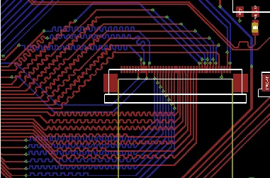
FR4 PCB Differential Pair Routing: Spacing and Length Matching
Intra-pair gap sets Zdiff on FR4; length matching does not fix an uncoupled route. Gap rules, delay match, and routing errors that still pass DFM.


