


PCB Design
Printed Circuit Board (PCB) design forms the backbone of modern electronics, enabling the creation of compact, efficient, and reliable devices that power everything from smartphones to industrial machinery. In this category, readers gain access to a comprehensive collection of resources dedicated to mastering PCB design principles and techniques. Whether you are a seasoned engineer refining complex layouts or a newcomer learning the fundamentals, these articles provide the knowledge needed to tackle real-world challenges in electronics development. The scope of PCB design covered here extends from initial schematic capture to final board fabrication and testing. Articles delve into essential topics such as layer stacking, signal integrity, thermal management, and component placement strategies. Guides and tutorials offer step-by-step instructions for using popular software tools like Altium Designer and KiCad, while insights explore emerging trends like flexible PCBs and high-speed designs. Best practices emphasize error reduction, cost optimization, and compliance with industry standards, ensuring designs are not only functional but also manufacturable at scale. Real-world applications highlight the category's practical value, demonstrating how effective PCB design contributes to innovations in automotive systems, medical equipment, renewable energy solutions, and consumer gadgets. By addressing common pitfalls and sharing expert tips, these pieces equip professionals to enhance product performance and reliability. Readers benefit from building a deeper understanding through interconnected articles that cover foundational concepts alongside advanced methodologies, fostering continuous improvement in electronics projects. For those involved in prototyping or production, the technical relevance of this content lies in its focus on efficiency and innovation. Detailed discussions on impedance control, EMI shielding, and design for manufacturability prepare you to meet the demands of today's fast-paced tech landscape. Engaging with multiple articles in this category allows for a progressive learning path, where foundational knowledge supports exploration of specialized topics, ultimately leading to more robust and innovative PCB designs.
Featured Blog
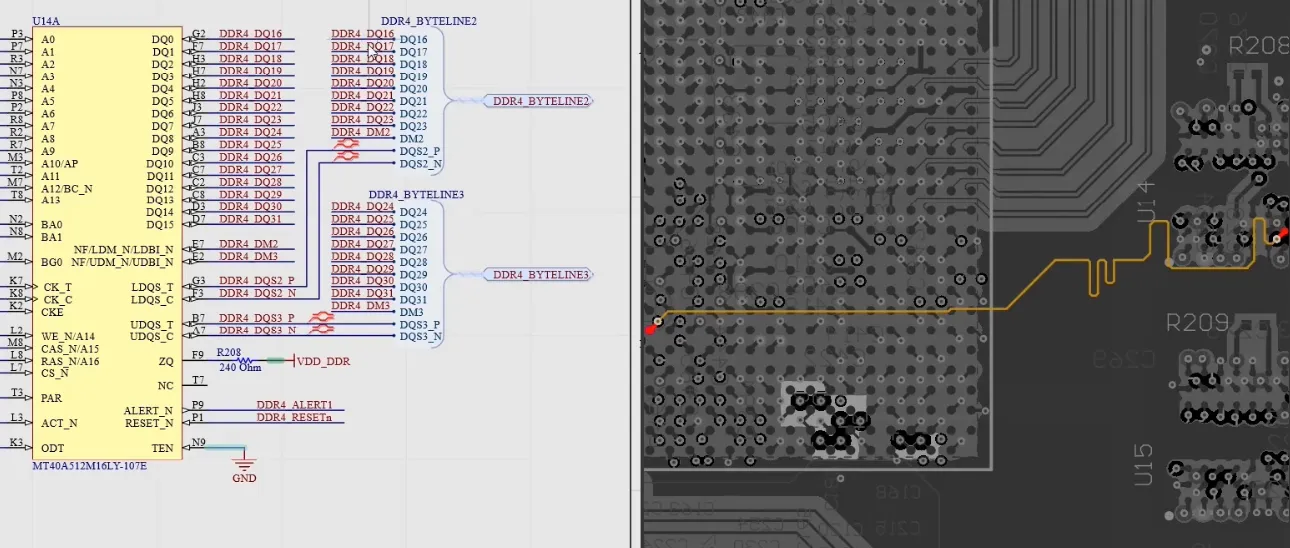
PCB Design Review for Beginners: A Step by Step Guide
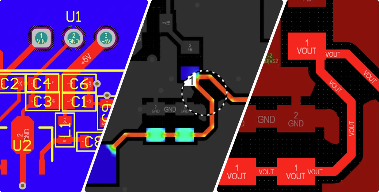
Learn how to perform a PCB design review with a practical checklist covering schematics, layout, DRC, manufacturability, and pre-production checks.
Latest Blogs
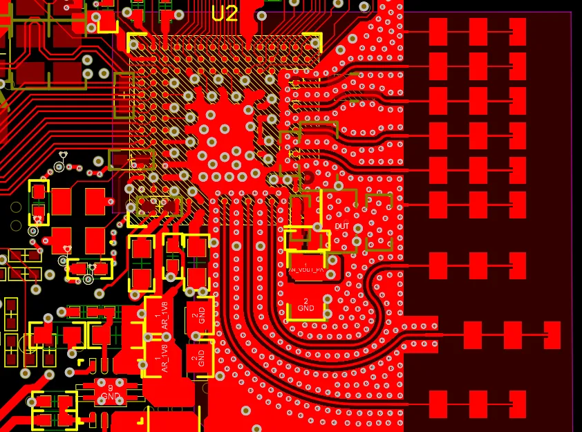
Signal-Integrity Simulation: Five Places Designs Usually Break
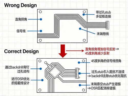
SI reports fail on hardware when time and frequency domains are split, eyes are judged only by opening, PDN ignores impedance, right-angle corners stay, or via stubs are left long.
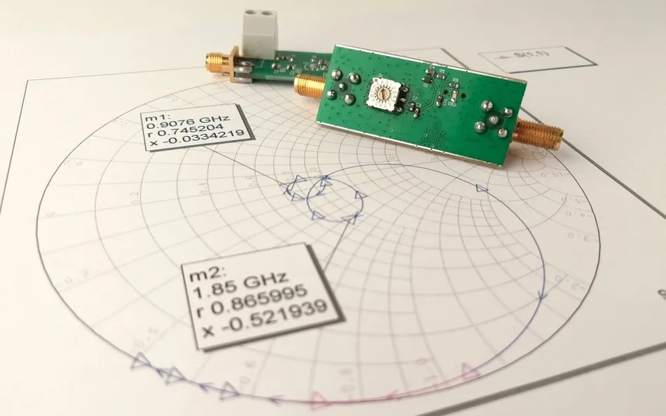
DC-DC Power-Module PCB Layout: 10 Rules That Usually Decide the Result
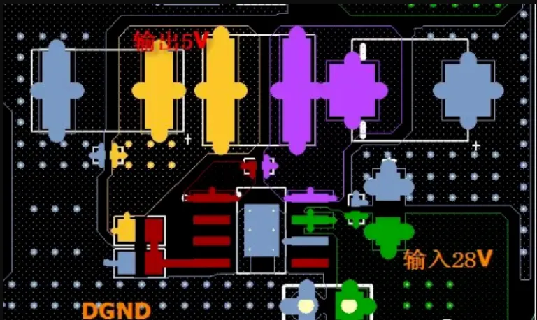
DC-DC failures are often layout: follow the datasheet, keep the power loop short, sense at the output cap, split AGND/PGND, and use thermal vias and pad reliefs.
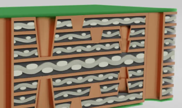
Random Routing Wastes the Board. These Layout Rules Come First
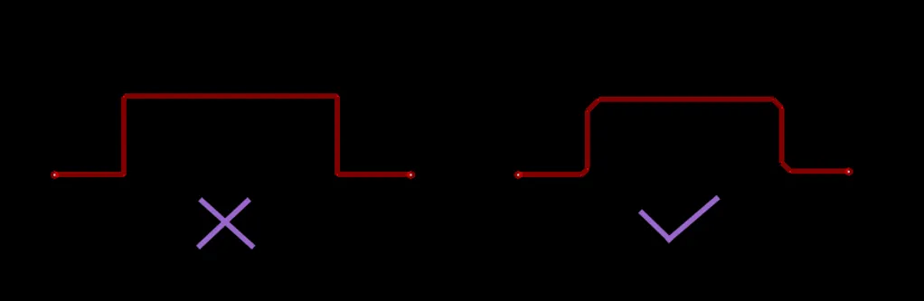
Route critical and dense nets first. Use 3W spacing, orthogonal layers, small return loops, no stubs or right angles, and keep impedance-controlled traces off plane splits.
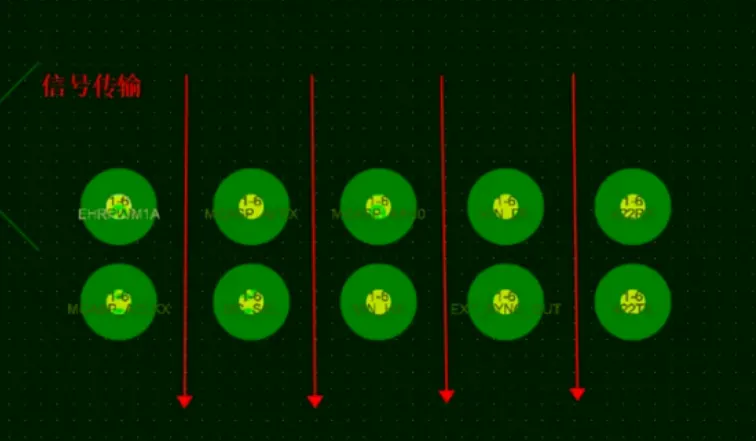
High-Speed PCB Vias: A Small Feature That Can Break the Signal
High-speed vias cause reflection, delay, and EMI when the return path is long or vias slot the plane. Place nearby ground vias and keep via spacing from fracturing copper.
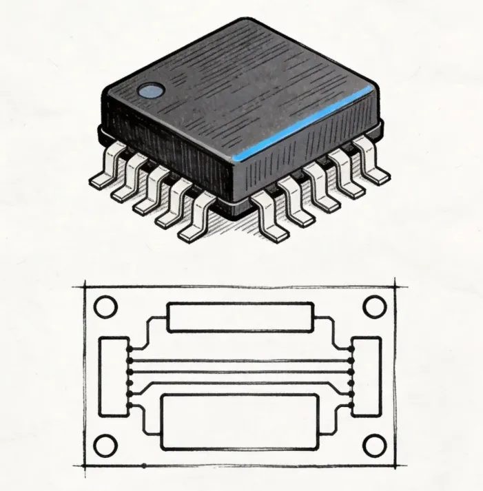
LDO Running Hot? Four Layout Practices That Matter
Cut LDO ripple and temperature with input/output caps at the pins, a single-point ground, ≥1 oz thermal copper with a via array, and infrared plus ripple checks.
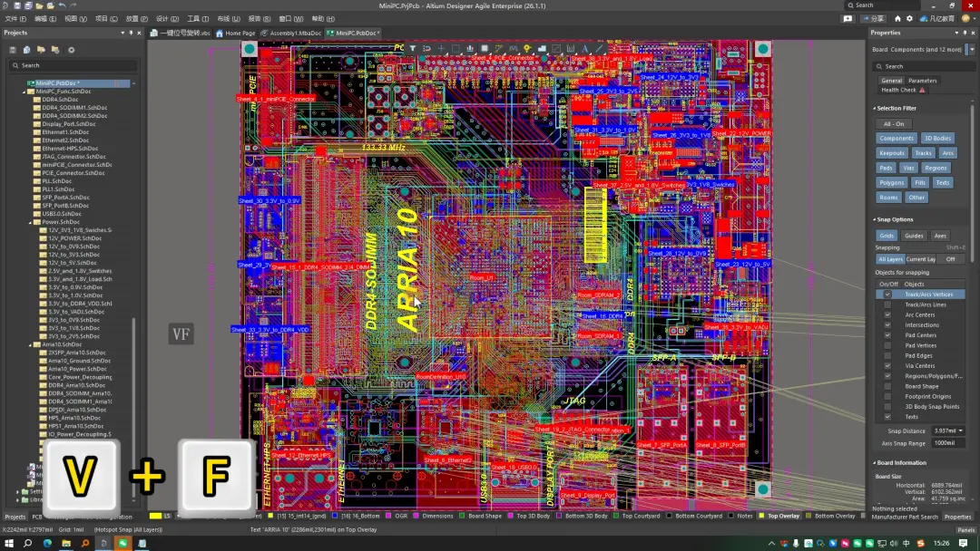
Nine Altium Designer Shortcuts That Cut PCB Drawing Time
VF, Shift+S, V+B, Ctrl+W, P+L, keypad +/−, Q, Ctrl+M, and middle-button zoom cover view, layer, unit, routing, and measure tasks used all day in Altium Designer.
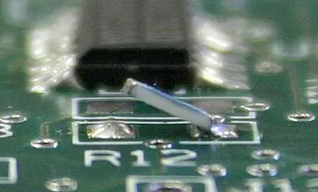
Can a Via Be Placed in a Pad? A Detail PCB Designers Cannot Skip
A via in a pad cuts lead inductance but can wick solder and tombstone chip parts. Pull the via off the pad and connect it with a short trace unless the hole is fully plugged.

Ten Beginner PCB Mistakes That Still Burn Boards
Default DRC, right-angle corners, distant decoupling, split planes, skinny power traces, silkscreen on pads, via-in-pad, and missing test points still wreck first boards.

Where High-Speed PCBs Usually Fail: Not Trace Width, but the Return Path
High-speed faults often come from a broken return path, not width error. Keep the reference plane continuous, bridge splits, and place return vias at layer changes.
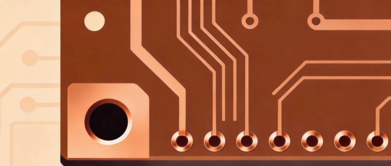
Via Inductance in PCB Design: Causes, Calculation & Reduction
A 1.0 mm via can add 1–2 nH and close a 5 GHz eye. Cut inductance with drill/pad rules, nearby return vias, back-drill, fewer layer changes, and 3D via simulation.
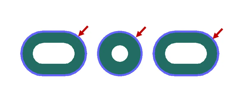
Why the Solder Mask Bridge Disappears Even When There Is a Gap Between Pads
A copper gap does not keep a solder mask bridge. Mask opening expansion, overlapping apertures, and fabricator dam limits decide whether the green dam survives.
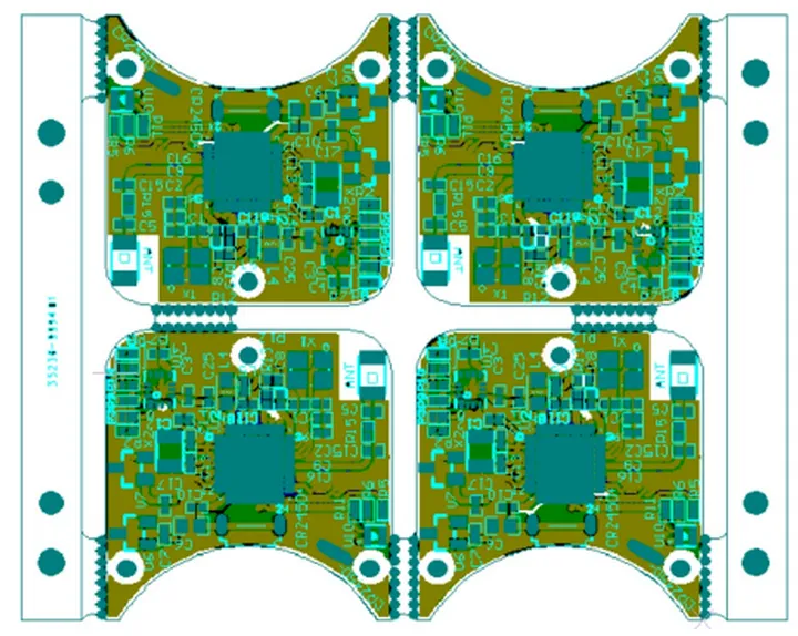
Why Adding Process Edges to a PCB Panel Is Not Wasted Board Material
Extra process edges on a PCB panel support transport, clamping, fiducials, and depaneling. See when they are required and how to check if they can be reduced.


