


PCB Design
Printed Circuit Board (PCB) design forms the backbone of modern electronics, enabling the creation of compact, efficient, and reliable devices that power everything from smartphones to industrial machinery. In this category, readers gain access to a comprehensive collection of resources dedicated to mastering PCB design principles and techniques. Whether you are a seasoned engineer refining complex layouts or a newcomer learning the fundamentals, these articles provide the knowledge needed to tackle real-world challenges in electronics development. The scope of PCB design covered here extends from initial schematic capture to final board fabrication and testing. Articles delve into essential topics such as layer stacking, signal integrity, thermal management, and component placement strategies. Guides and tutorials offer step-by-step instructions for using popular software tools like Altium Designer and KiCad, while insights explore emerging trends like flexible PCBs and high-speed designs. Best practices emphasize error reduction, cost optimization, and compliance with industry standards, ensuring designs are not only functional but also manufacturable at scale. Real-world applications highlight the category's practical value, demonstrating how effective PCB design contributes to innovations in automotive systems, medical equipment, renewable energy solutions, and consumer gadgets. By addressing common pitfalls and sharing expert tips, these pieces equip professionals to enhance product performance and reliability. Readers benefit from building a deeper understanding through interconnected articles that cover foundational concepts alongside advanced methodologies, fostering continuous improvement in electronics projects. For those involved in prototyping or production, the technical relevance of this content lies in its focus on efficiency and innovation. Detailed discussions on impedance control, EMI shielding, and design for manufacturability prepare you to meet the demands of today's fast-paced tech landscape. Engaging with multiple articles in this category allows for a progressive learning path, where foundational knowledge supports exploration of specialized topics, ultimately leading to more robust and innovative PCB designs.
Featured Blog
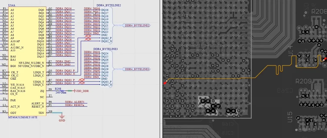
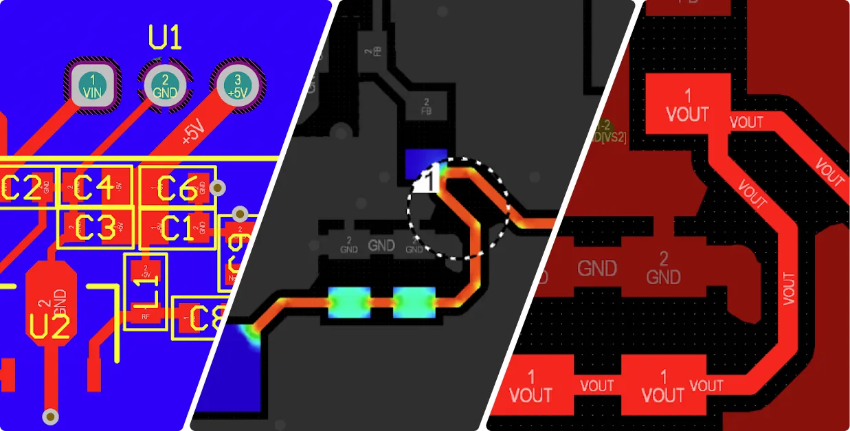
PCB Design Review for Beginners: A Step by Step Guide
Learn how to perform a PCB design review with a practical checklist covering schematics, layout, DRC, manufacturability, and pre-production checks.
Latest Blogs
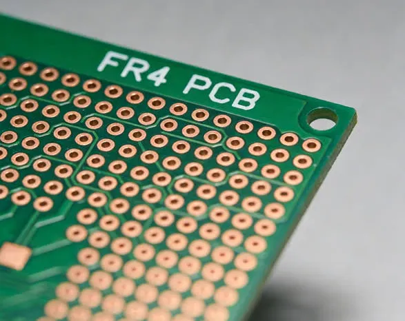
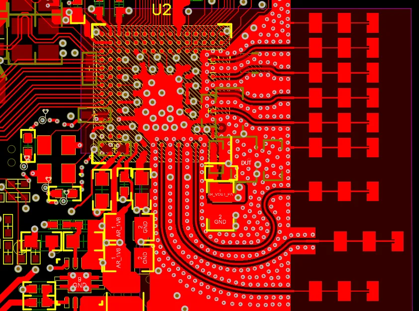
FR4 PCB Controlled Impedance: When Do You Need It?
When FR4 PCB controlled impedance is actually required: which high-speed nets need a target Z0, why a 1.6 mm two-layer stack cannot hit 50 Ω at signal widths, and how fab meets the number with stackup, etch compensation, and coupons.
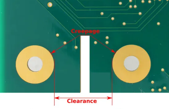
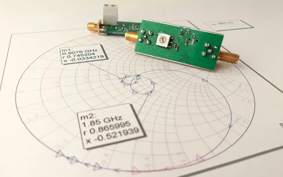
FR4 PCB Creepage vs Clearance: Design Rules for High-Voltage Boards
FR4 PCB creepage vs clearance are not the same spacing rule. Set creepage and PCB clearance high voltage from working voltage, CTI, and pollution degree—not one CAD gap.
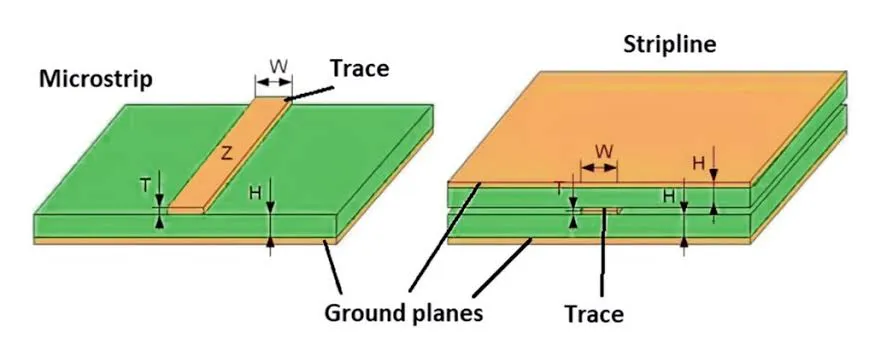
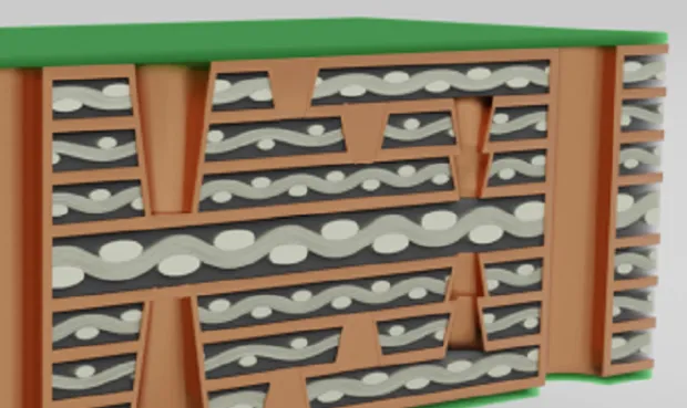
FR4 PCB Length Matching: When It Matters and How to Design It
Learn when FR4 PCB length matching is required based on propagation delay. Covers interface tolerances, serpentine design rules, and practical PCB trace length matching guidelines for high-speed signals.
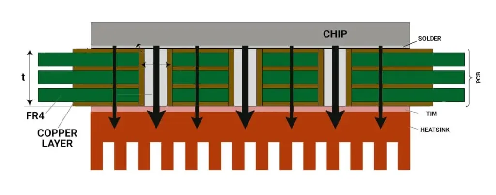
FR4 PCB Thermal Via Design for High-Power Components
Practical FR4 PCB thermal via design for high-power components. Covers heat path, optimal via count, pitch limits, copper plane continuity and thermal resistance optimization to avoid overheating on standard FR4 boards.
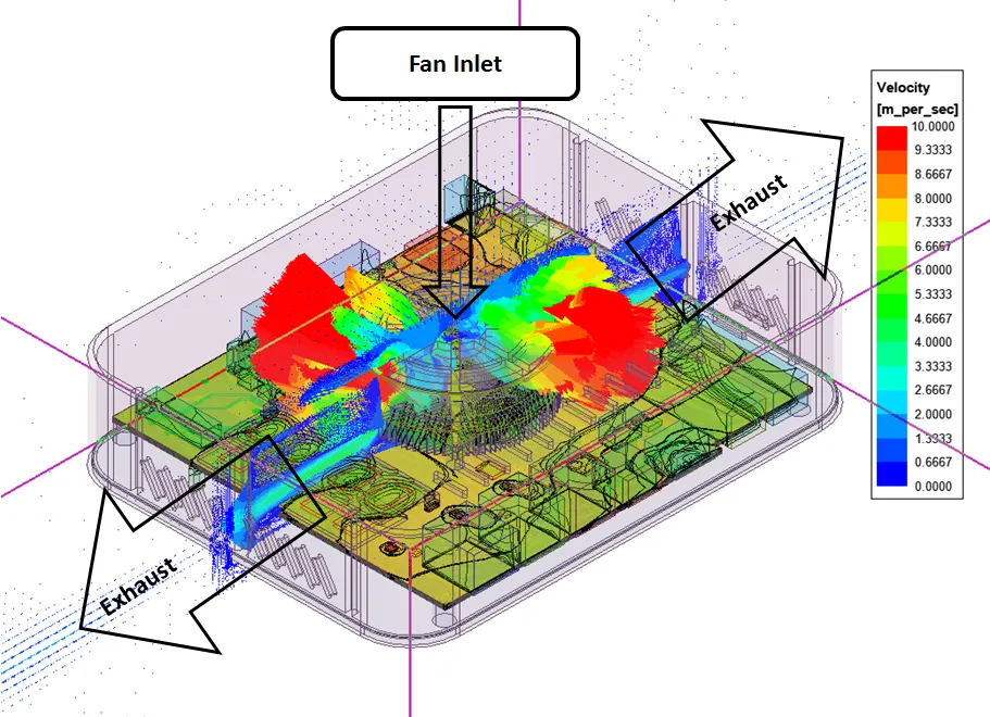
FR4 PCB Component Placement for Better Thermal Performance
Learn FR4 PCB component placement thermal rules: identify heat sources, set spacing, build copper spreading paths, and place high-power parts without hot islands. Practical PCB thermal component placement guidance.
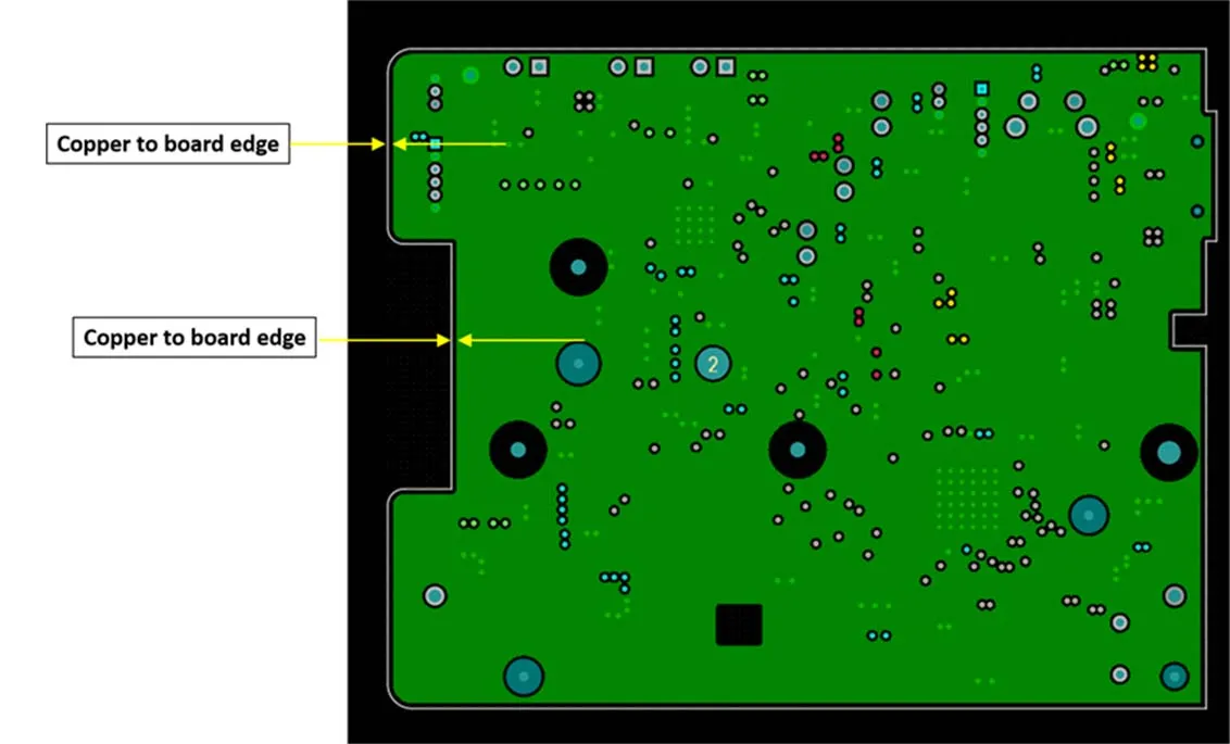
FR4 PCB Edge Clearance: How Much Copper Should Be Kept from the Board Edge?
FR4 PCB edge clearance defines how far copper must stay from the finished board edge. Covers routing tolerance, exposed-copper shorts, depanel stress, and safe copper-to-board-edge spacing on standard FR4.
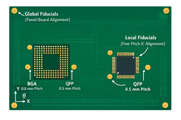
FR4 PCB Fiducial Design: Placement Rules for Reliable Assembly
Learn FR4 PCB fiducial design rules for reliable SMT: global vs local marks, size and clearance, camera recognition, and PCB fiducial placement errors that cause misalignment.
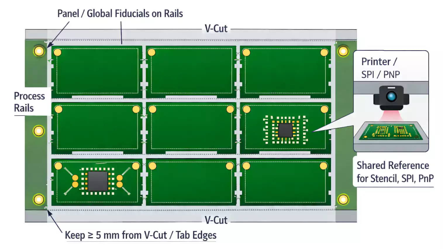
FR4 PCB Panelization Design: Fiducials, Rails, and Tooling Holes
FR4 PCB panelization design for production: rail width, fiducial size and placement, tooling hole specs, and when to use V-score versus routed tabs so SMT panels locate, hold, and depanel without damage.
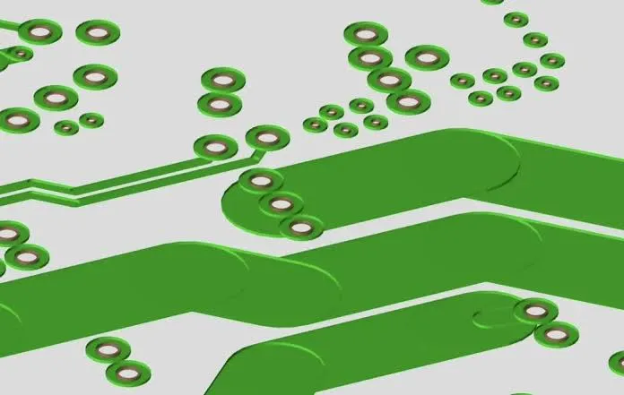
FR4 PCB Stitching Vias: When and Where to Use Them
Practical engineering notes on FR4 PCB stitching vias—when plane gaps force them, recommended via spacing for EMI and return paths, board-edge clearance limits, and density constraints that affect manufacturability.
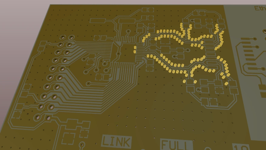
FR4 PCB Ground Via Placement: Best Practices for Signal Integrity
Practical rules for FR4 PCB ground via placement and ground stitching vias. Correct return-path spacing, common layout errors, and density guidelines that protect high-speed signal integrity.

FR4 PCB Thermal Vias: Placement and Design Guidelines
Practical FR4 PCB thermal via design rules: via count and pitch, under-pad placement, copper path continuity, and fabrication limits that control real heat transfer and long-term reliability.
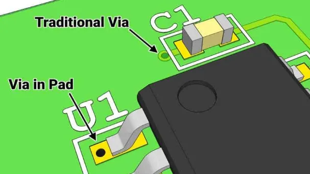
FR4 PCB Via-in-Pad: Benefits, Risks, and Design Considerations
FR4 PCB via in pad reduces routing space and improves thermal paths, but open barrels cause solder wicking and starved joints. Covers resin fill requirements, cap plating, assembly risks, and when the process is justified versus dogbone or microvia alternatives.


