


PCB Manufacturing
Printed Circuit Boards (PCBs) form the backbone of modern electronics, serving as the essential platform where components connect to create functional devices. In the PCB Manufacturing category, readers gain access to a comprehensive collection of resources designed to demystify the intricate processes involved in producing these critical elements. From initial design considerations to final assembly and testing, this category covers every stage, providing valuable insights for engineers, hobbyists, and industry professionals alike. Understanding PCB manufacturing is crucial for anyone involved in electronics development. This field encompasses a wide range of topics, including material selection, such as FR-4 substrates and advanced laminates, as well as fabrication techniques like etching, drilling, and soldering. Articles here delve into best practices for optimizing layouts to minimize signal interference, ensuring reliability in high-stakes applications. Tutorials guide users through prototyping methods, while in-depth analyses explore emerging trends like flexible PCBs and additive manufacturing, which are revolutionizing industries from consumer gadgets to aerospace systems. The practical value of mastering PCB manufacturing extends to real-world scenarios, where efficient production can reduce costs, enhance performance, and accelerate time-to-market. For instance, insights on multilayer board construction help in designing compact devices for IoT applications, and discussions on quality control standards prevent common pitfalls in mass production. By engaging with the diverse guides and expert perspectives in this category, readers can build a solid foundation in PCB technologies, apply proven strategies to their projects, and stay ahead in an ever-evolving field. Whether troubleshooting assembly issues or exploring sustainable manufacturing practices, the knowledge shared here empowers informed decision-making and innovation in electronics.
Latest Blogs
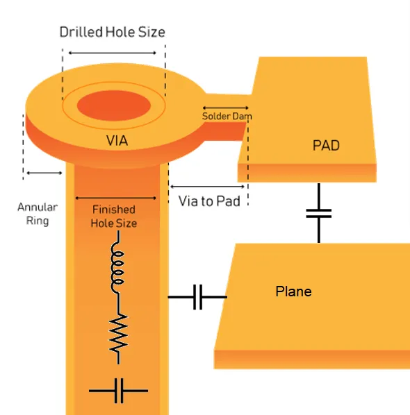
The Ultimate Guide to Via Design for Signal Integrity: Optimizing Aspect Ratios for High Speed PCBs
Optimize via aspect ratio signal integrity in high-speed PCBs to cut parasitic inductance via and via capacitance effects. This guide covers high-speed PCB via design, microvia vs buried via signal integrity, and best practices for engineers to achieve clean signals and reliable boards.
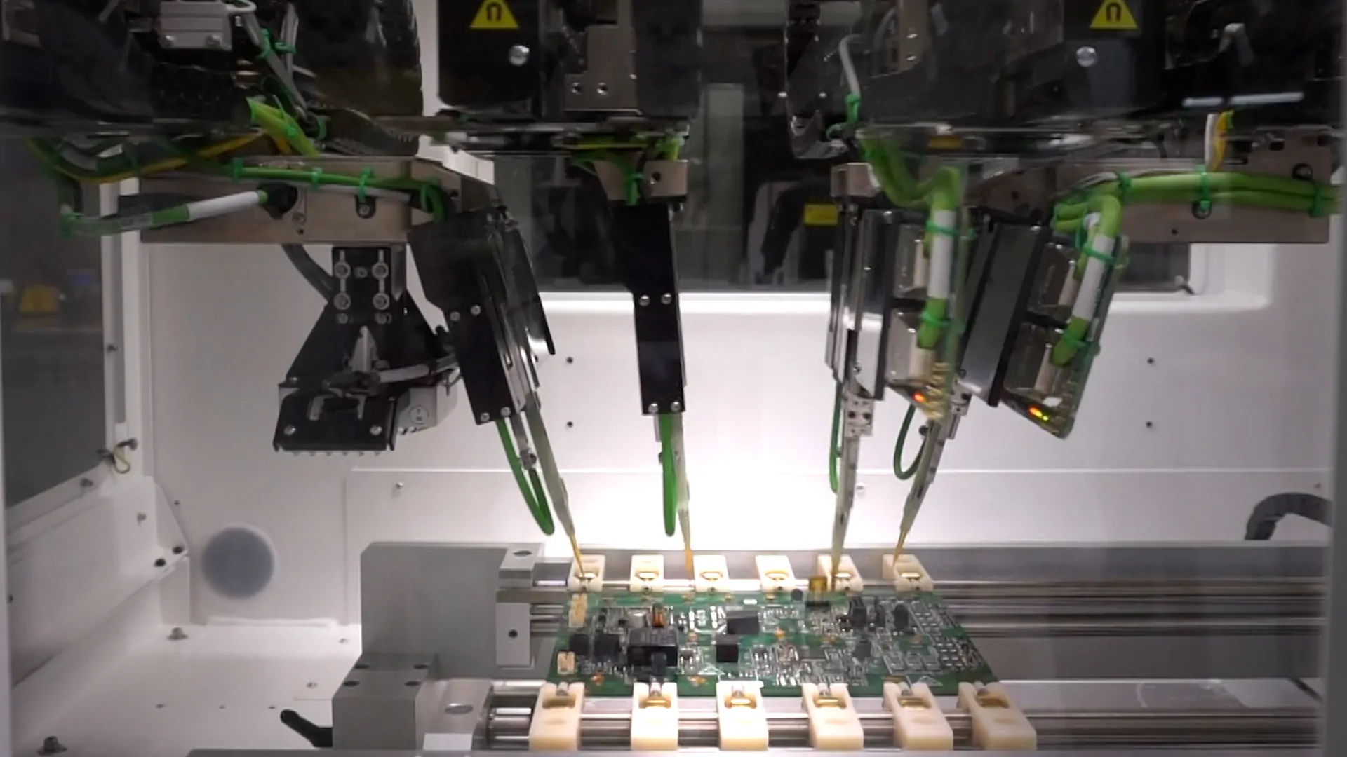
Boosting PCB Reliability: How Flying Probe Testing Minimizes Manufacturing Defects
Flying probe testing provides precise defect detection for PCB manufacturing, catching opens, shorts, and parametric issues to boost reliability. Fixtureless design suits prototypes and low volumes. Details include technical principles, comparisons to bed-of-nails, best practices per IPC standards, and FAQs on FPT for quality control. (197 characters)

DFM for Signal Integrity: How Early Collaboration with Manufacturers Prevents Costly Reworks
Early manufacturer collaboration in PCB design for manufacturability signal integrity avoids common signal integrity issues in manufacturing and slashes PCB rework costs. Electric engineers get a practical PCB design review checklist, best practices, and troubleshooting insights for first-pass high-speed PCB success.
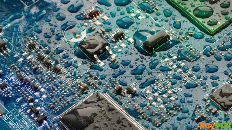
Acrylic Conformal Coating: The Go To Choice for Hobbyists and Professionals Alike
Acrylic conformal coating protects hobby electronics from moisture, dust, and wear. Key properties include flexibility and dielectric strength. Follow step-by-step applying acrylic conformal coating tips, easy removal methods, and best practices for reliable hobby projects. Ideal for sensors, drones, and prototypes. (187 characters)
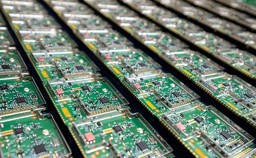
Epoxy Conformal Coating: When You Need Unmatched Chemical and Abrasion Resistance
Epoxy conformal coating properties offer top chemical and abrasion resistance for PCBs in industrial environments. Details on application methods, removal techniques, and best choices for harsh chemicals help electric engineers protect circuits effectively in demanding conditions. (187 characters)
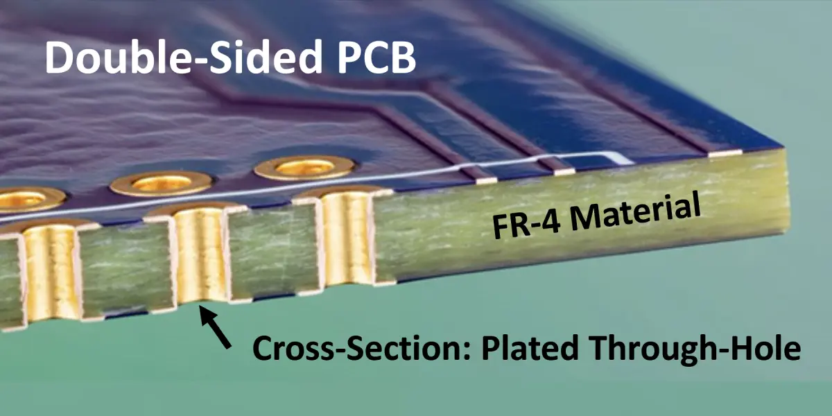
Double Sided PCB Materials Face Off: FR 4 vs. Alternatives
Compare FR-4 double-sided PCB with alternatives like polyimide and ceramics for high-temperature needs. Review thermal conductivity, CTE, cost factors and best practices for electric engineers to select materials that ensure reliability and manufacturing success in demanding applications.
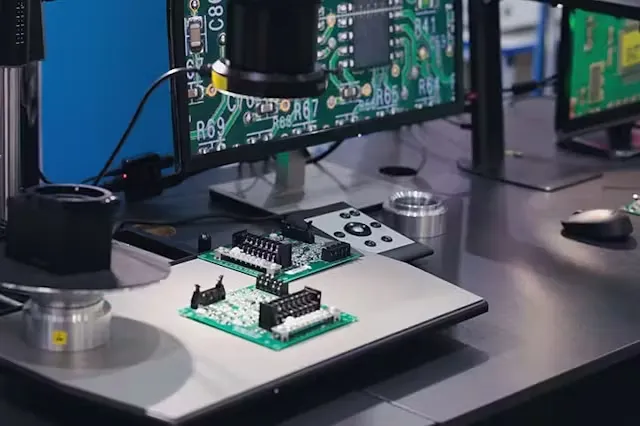
PCB Manufacturing for Beginners: A Step by Step Guide to Getting Your Boards Made
Follow this beginner guide to the PCB manufacturing process for hobbyists. Learn about Gerber files, key specifications, choosing a manufacturer, and ordering PCBs online for affordable prototypes. Get boards made right the first time with practical tips and best practices.
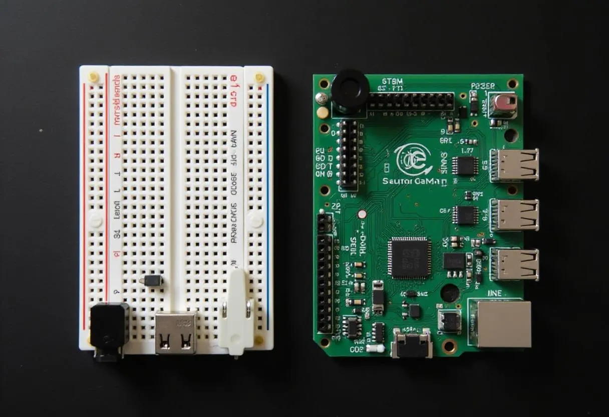
From Breadboard to PCB: Making Your Projects Permanent
Discover the complete process from breadboard to PCB and make your electronics permanent, compact, and reliable. This guide shows hobbyists how to design from schematic, use the toner transfer method, and perform DIY PCB etching for professional results at home.
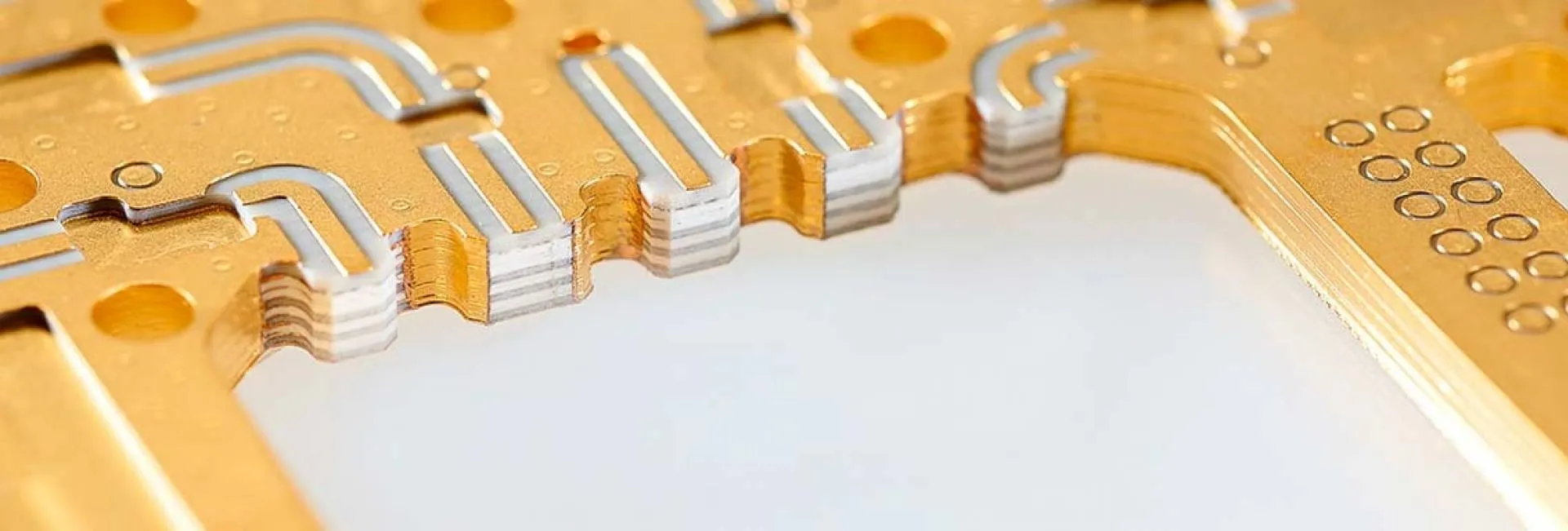
Exploring the Benefits of Multi Layer PTFE PCBs for Complex Designs
Multilayer PTFE PCBs enable high density interconnects and precise routing for complex high frequency designs. Low dielectric loss and thermal stability support RF telecom and digital circuits over 10 GHz. Best practices include stack up optimization via strategies and impedance testing for reliable performance.
Troubleshooting Common Issues in PTFE PCB Assembly
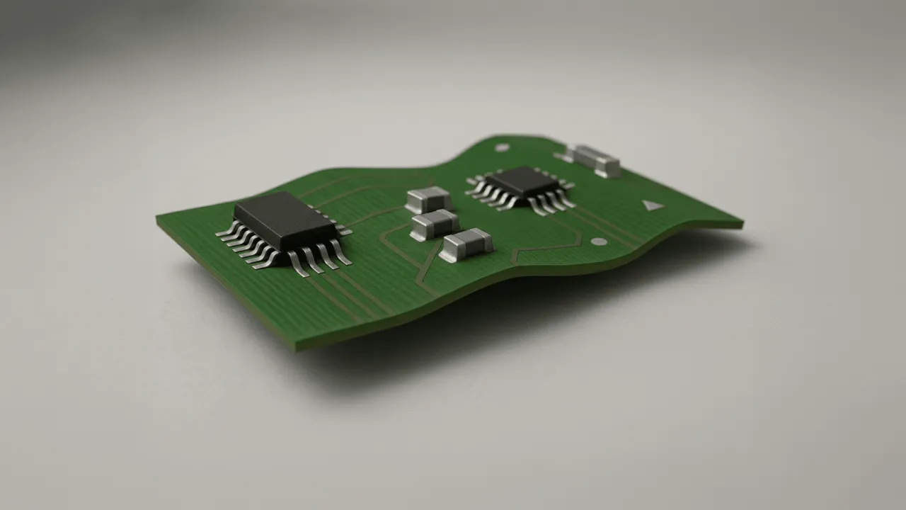
Electrical engineers guide to fixing PTFE PCB solderability problems, component placement errors, and reflow process challenges. Get practical troubleshooting steps, best practices, and standards like IPC J-STD-001 for reliable high-frequency assemblies and higher yields.
Mastering Impedance Control in PTFE PCB Manufacturing: A Step by Step Guide
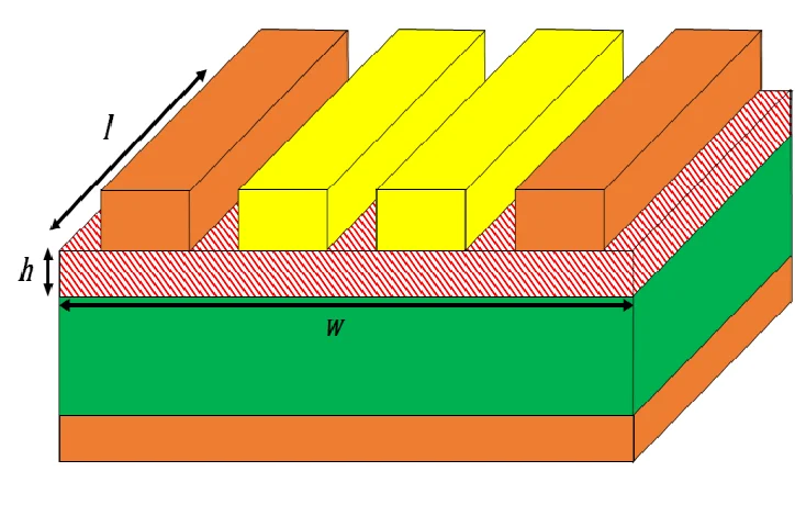
Step by step guide to PTFE PCB controlled impedance in manufacturing. Learn laminate selection, stackup design, trace geometry, process controls, and TDR testing for precise PTFE PCB transmission lines and signal integrity in high frequency applications. Ideal for electrical engineers.
Small Batch PCB Manufacturing: Revolutionizing Rapid Prototyping for IoT Devices
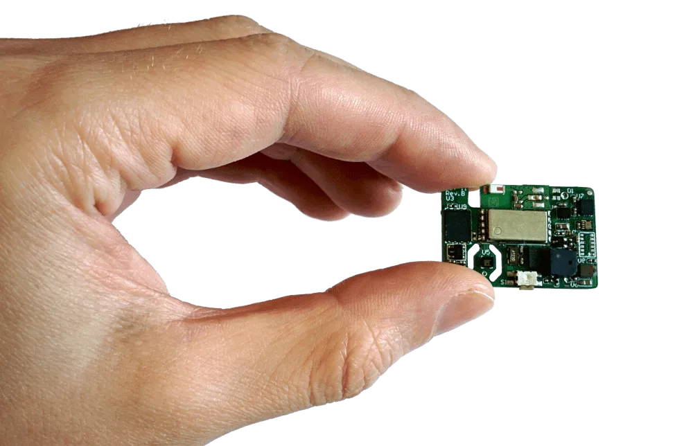
Small batch PCB manufacturing quickens rapid prototyping for IoT devices with low volume runs. Electric engineers find tips on iot pcb design, low power pcb manufacturing, pcb for wireless sensors, iot device prototyping, and connected device pcb assembly. Streamline workflows and boost prototype reliability using industry standards.


