 01:02
01:02
PCB Copper Pour
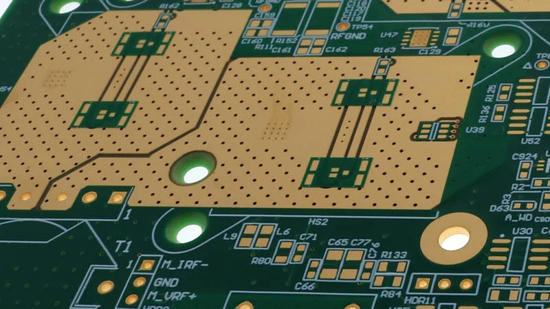
PCB copper pour is a fundamental technique in printed circuit board design that involves filling unused areas of the board with copper to create ground planes, improve heat dissipation, or enhance signal integrity. For engineers and hobbyists searching for information on PCB copper pour, this tag serves as a comprehensive resource, gathering articles that delve into its implementation, benefits, and potential pitfalls. By understanding how to effectively apply copper pours, designers can minimize electromagnetic interference, reduce noise in high-speed circuits, and ensure more reliable performance in complex layouts. In practice, PCB copper pour is particularly valuable for multilayer boards where it helps in creating solid ground references and thermal vias to manage heat from power-intensive components. Best practices include maintaining adequate clearance from traces to avoid shorts, using stitching vias for better connectivity across layers, and optimizing pour shapes to prevent isolated copper islands that could act as antennas for unwanted signals. For instance, in RF designs, a well-executed copper pour can significantly lower impedance and improve shielding, while in power electronics, it aids in even current distribution to prevent hotspots. Users often arrive here seeking guidance on tools like KiCad or Eagle for automating pours, troubleshooting issues such as thermal relief connections, or integrating pours with other design elements like polygons and keep-out zones. The articles linked under this tag offer step-by-step tutorials, case studies, and expert tips to help you refine your PCB projects. Whether you are optimizing a prototype or scaling up for production, exploring these resources can provide the insights needed to elevate your designs from functional to exceptional.
Video Guide
-
01:02
Technical Articles

Should You Use Solid or Hatched Copper Pour on PCBs?
PCB CAM Review to Overcome Complex Stackup and Lamination Challenges
PCB CAM Review for Copper and SMD Pads Near the Board Edge
Common PCB Design Pitfalls and How to Avoid Them

Adding Via Stitching in KiCad with the kicad-action-scripts Plugin

Precise Spacing Control: How to Move a Diagonal Feature by Exactly 1 mm
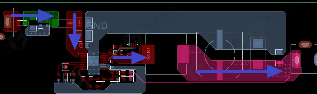
PCB Layout and Routing for Switching Regulators and LDOs: A Practical Guide

Do You Need a Full-Board Copper Pour on Your PCB?
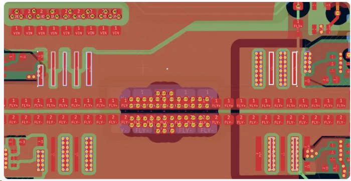
Fill Resistance Plugin: Measured Copper Pour Resistance and PDN Voltage Drop
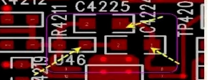
Power Module PCB Design: From Theory to Practice
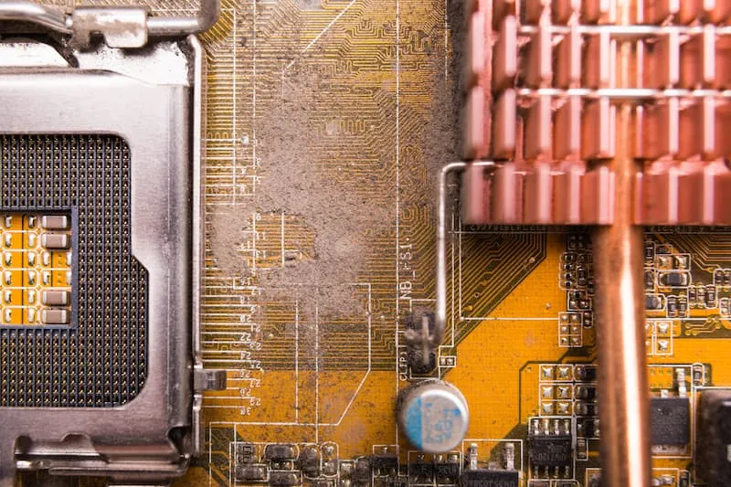
Why Your PCB Keeps Having Problems: You May Have Chosen the Wrong Copper Pour
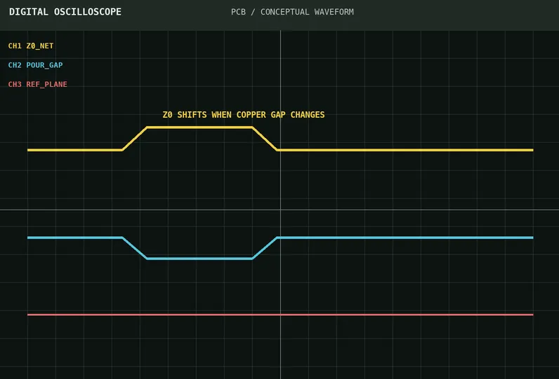
Why Impedance Changes After Adjacent Copper Pour Even When Trace Width Does Not
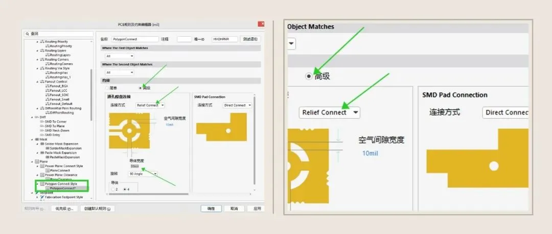
Why Does a Pad Tied Straight to a Copper Pour Become More Prone to Poor Soldering?
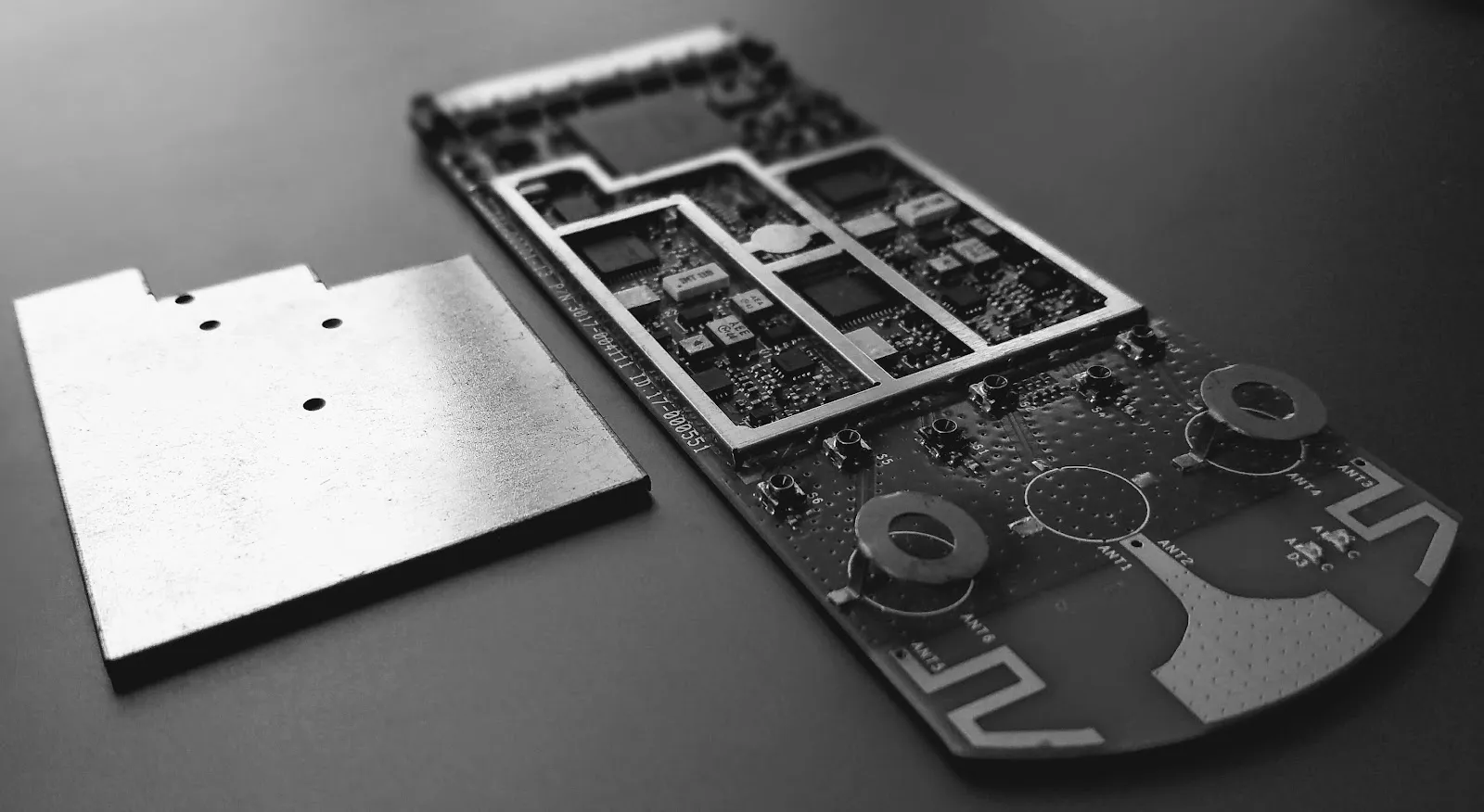
The Case For Using Copper Pour On Routing Layers
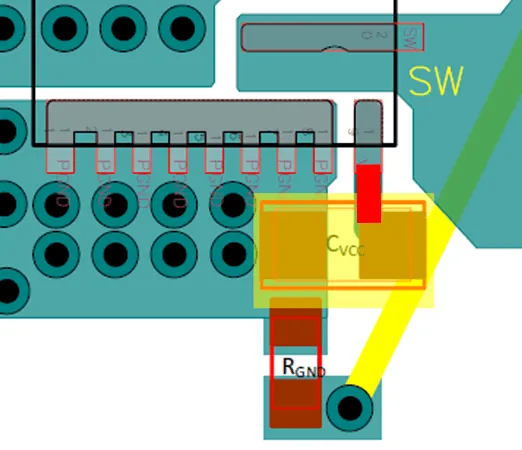
Key PCB Layout Guidelines for Buck Converters
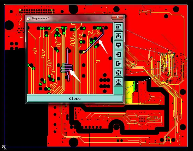
How DFM Review Secured Impedance Control in 6-Layer FR4 PCB
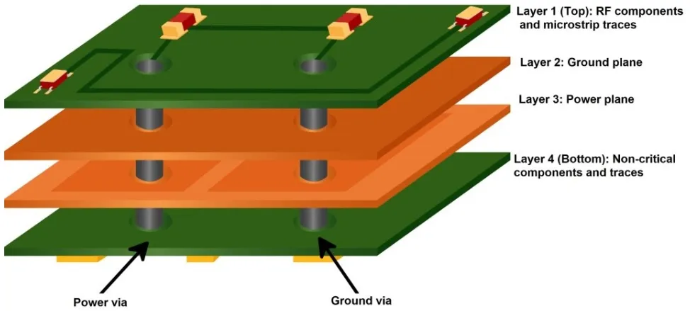
Demystifying Inner Layer Copper Pouring for Hobbyist PCBs

DIY Guide: Modifying Outer Layer Copper Thickness for Improved Thermal Performance in Custom PCBs
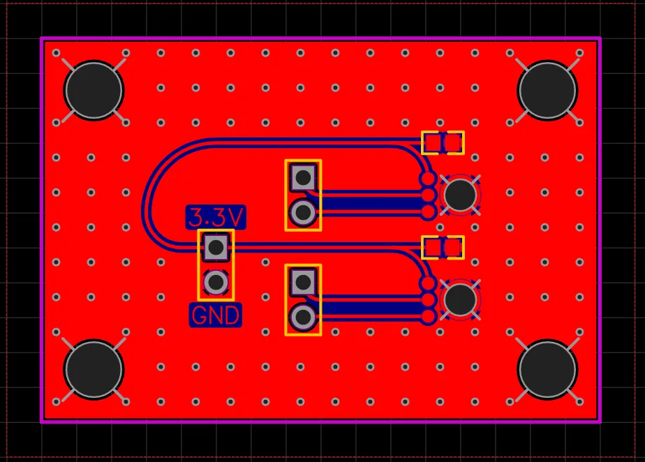
Mastering PCB Copper Pour: Techniques for Effective Grounding and Noise Reduction