 19:28
19:28
PCB Design Review
PCB design review is a critical step in the electronics development process, ensuring that printed circuit board layouts meet functional, manufacturing, and reliability standards before production. For engineers, designers, and hobbyists searching for guidance on PCB Design Review, this tag serves as a comprehensive resource to identify and mitigate potential issues early, reducing the risk of costly revisions or failures in the field. By focusing on systematic evaluation techniques, such as checking for signal integrity, power distribution, and component placement, users can achieve designs that perform optimally under real-world conditions. Key aspects covered under this tag include best practices for conducting thorough reviews, from initial schematic validation to final Gerber file inspections. Practical applications often involve tools like simulation software for thermal analysis and EMC compliance, helping to spot common pitfalls such as inadequate trace widths or overlooked grounding strategies. These insights are particularly valuable for those aiming to streamline their workflow, whether prototyping a new device or scaling up for mass production. Implementing a structured review checklist can significantly enhance design quality, ensuring adherence to industry standards like IPC guidelines and minimizing defects that could lead to product recalls. For deeper understanding, the articles here delve into case studies and step-by-step tutorials that demonstrate how to apply these principles in various scenarios, from consumer electronics to industrial applications. Readers interested in refining their skills will find value in exploring topics like automated design rule checks and peer review processes, which foster better collaboration and innovation in PCB projects.
Video Guide

Technical Articles

How PCB CAM Resolves Blind Via Size and Edge Clearance Issues
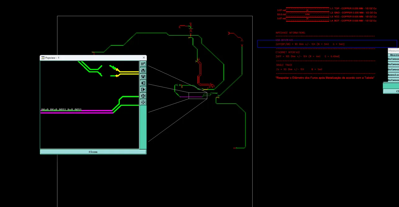
How PCB CAM Resolves Conflicting Impedance Control Requirements
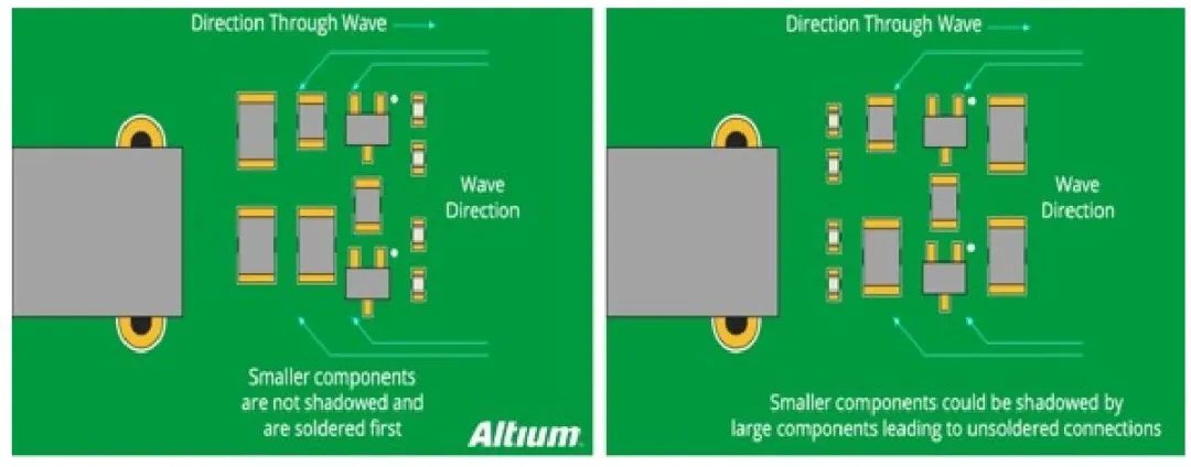
Six Practical PCB Design Techniques That Avoid Common Manufacturing Problems
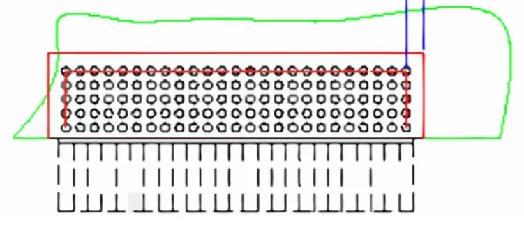
Why Moving a Component Only 1 mm from a Press-Fit Connector Still Causes Assembly Interference

Why Traces Can Still Open After Teardrops Are Added to Vias
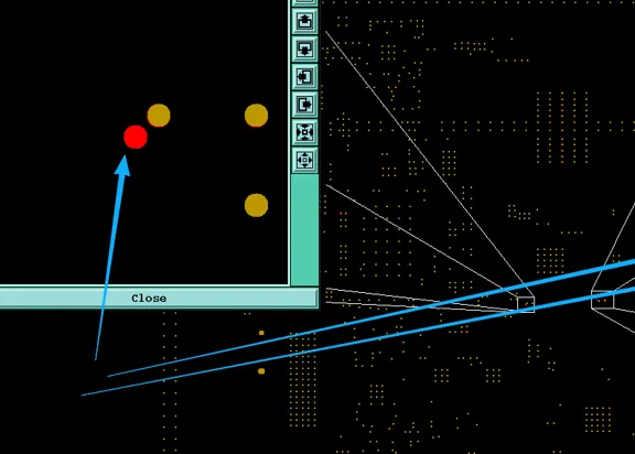
PCB CAM Review: Fix V-Cut & Via Spacing to Avoid Delays
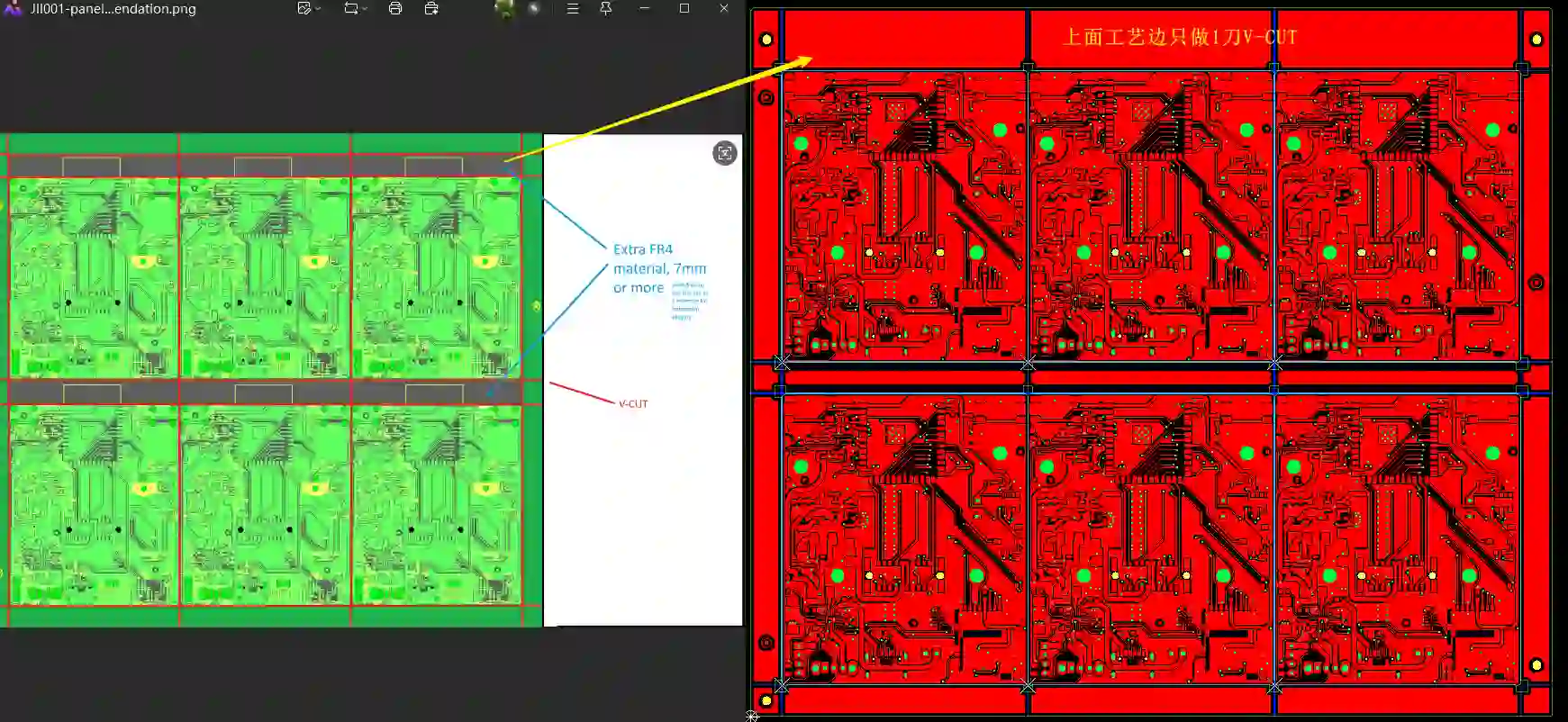
How to Solve 2-Layer PCB CAM Issues Before Manufacturing
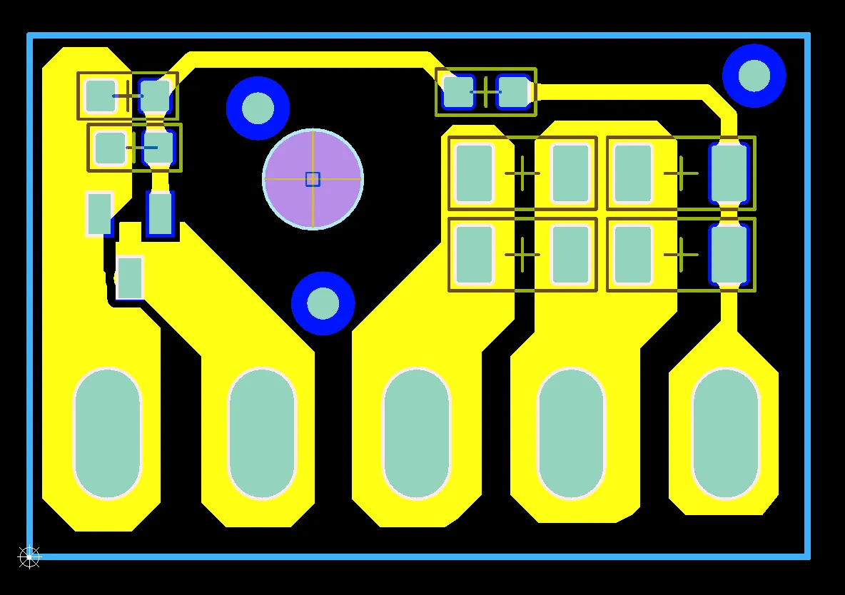
Common 1 Layer FR4 PCB EQ Issues: How Manufacturers Review Gerber Files

DFM for Signal Integrity: How Early Collaboration with Manufacturers Prevents Costly Reworks
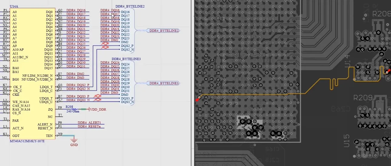
PCB Design Review for Beginners: A Step by Step Guide
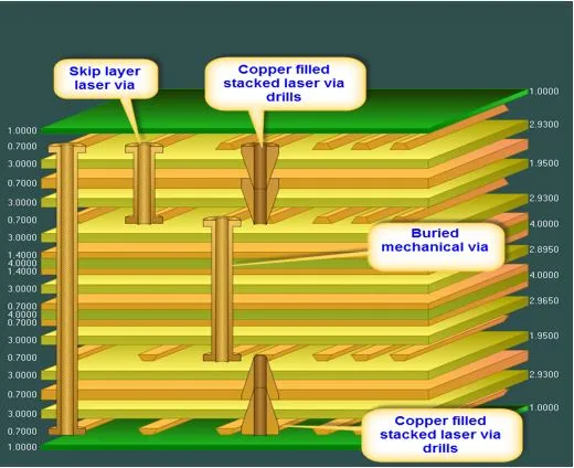
Avoiding Costly Mistakes: A Practical Guide to PCB Design Review
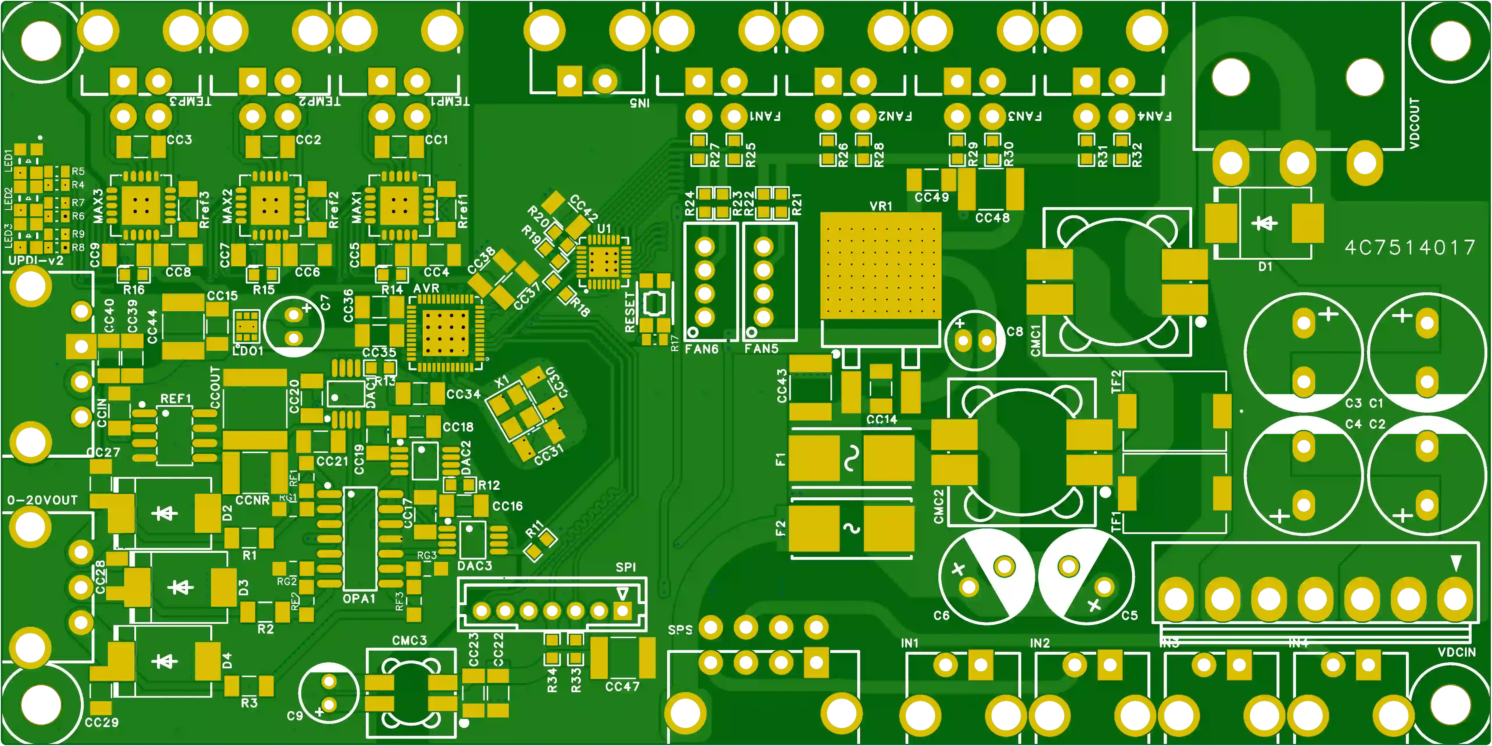
How Conflicting Via Data and Soldermask Definitions Triggered CAM Review in a 4-Layer HDI PCB
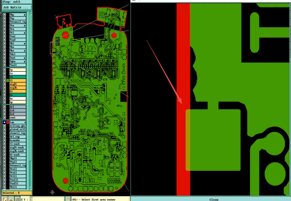
Engineering Case Study: 4-Layer 1.0mm FR-4 PCB Edge Clearance and Stamp Hole Spacing DFM Review

What Is KiCad? A Complete Introduction to Open Source PCB Design Software
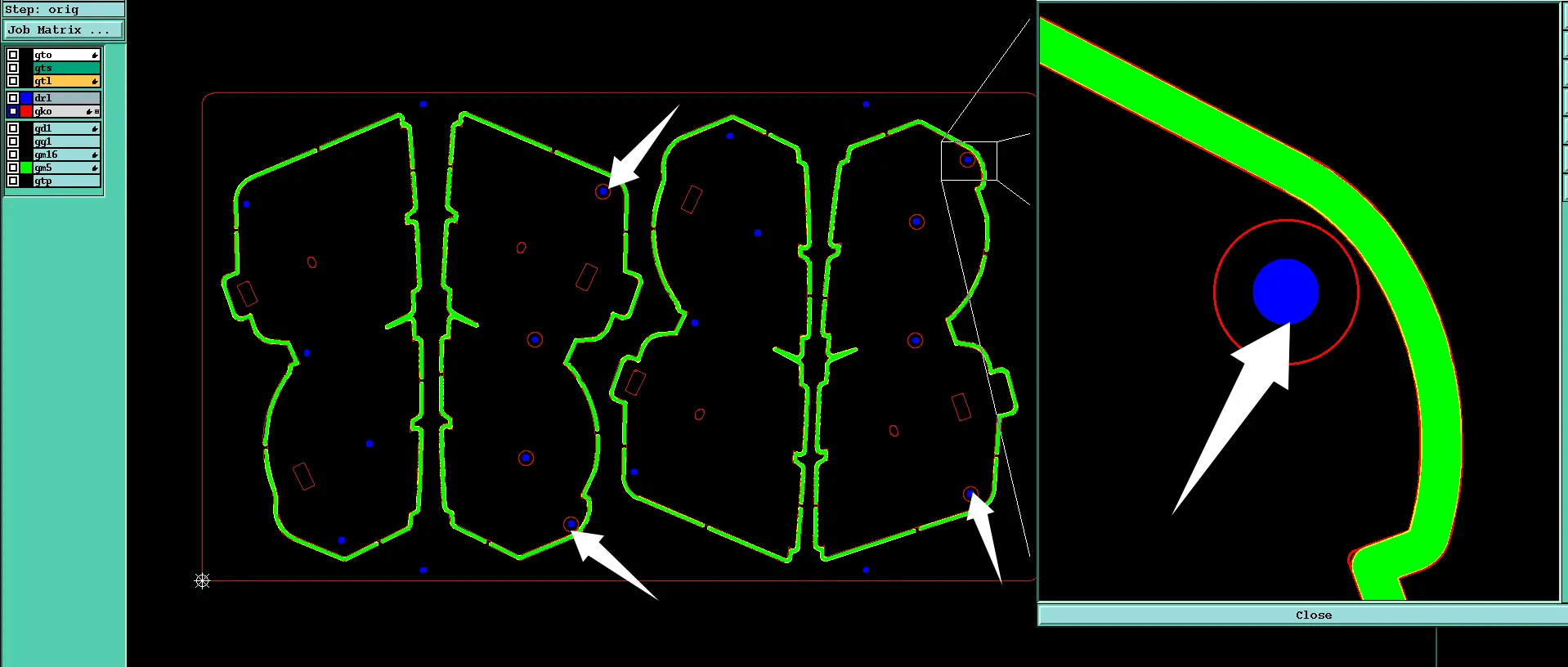
Aluminum PCB CAM Review: Avoiding Costly Drill-Outline Mistakes
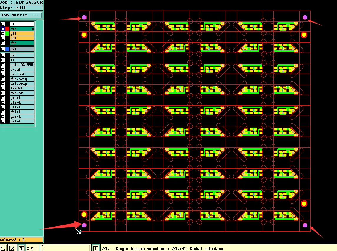
Tented Via vs Open Via Conflict Resolved in 2-Layer FR4 PCB
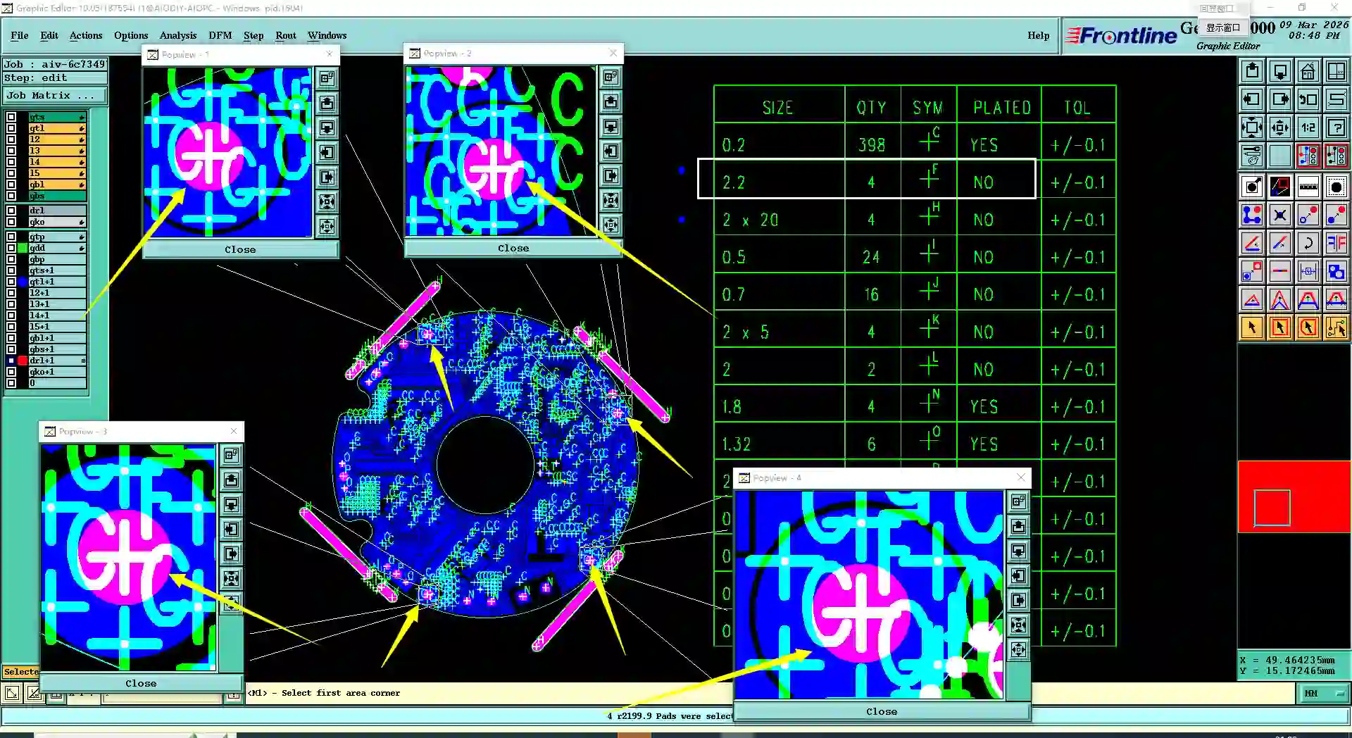
Why NPTH Hole with Pad Conflict Required Clarification Before 6-Layer Production
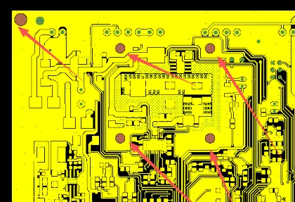
How to Fix 2 Layer FR4 PCB Design Errors During CAM Review
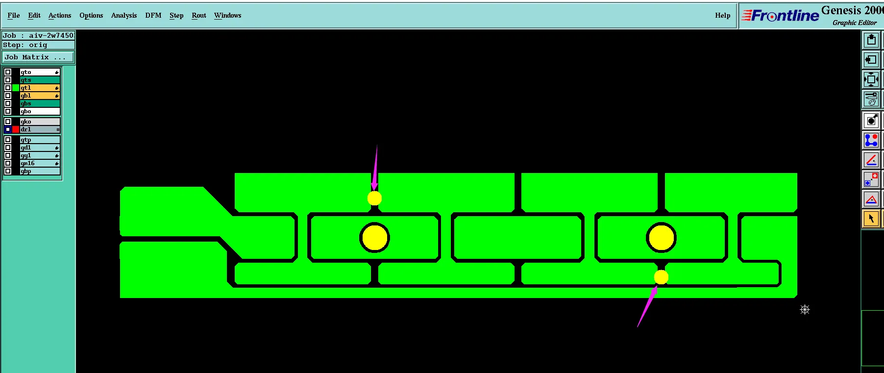
How Panelization Conflict Delayed Single Piece Delivery in 1-Layer PCB