PCB Thermal Design
Effective thermal management is a critical aspect of printed circuit board (PCB) design, ensuring that electronic components operate within safe temperature ranges to prevent failures, extend lifespan, and maintain performance. In the realm of PCB Thermal Design, engineers and designers focus on strategies to dissipate heat generated by high-power components, such as processors, power amplifiers, and LEDs. This involves selecting appropriate materials with high thermal conductivity, optimizing board layout for airflow, and incorporating features like thermal vias, heat sinks, and copper pours to enhance heat transfer. For those searching for PCB Thermal Design resources, this tag serves as a comprehensive hub for practical guidance tailored to real-world challenges. Whether you are troubleshooting overheating issues in consumer electronics, automotive systems, or industrial equipment, the content here delves into best practices that can be directly applied to your projects. Key topics include thermal simulation techniques using software tools like ANSYS or Altium, guidelines for multilayer board configurations to minimize thermal resistance, and case studies demonstrating how effective design choices have resolved common problems such as hot spots and thermal runaway. Understanding these principles not only helps in complying with industry standards like IPC-2152 for current-carrying capacity but also empowers you to innovate in designs that demand higher efficiency and reliability. By exploring the articles grouped under this tag, you can gain actionable insights into advanced methods, such as integrating phase-change materials or active cooling solutions, and learn from expert analyses of thermal modeling errors to avoid. This collection equips you with the knowledge to refine your PCB designs, ultimately leading to more robust and efficient electronic products.
Technical Articles

PCB Mass Production image
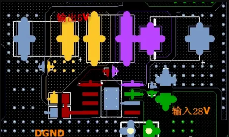
DC-DC Power-Module PCB Layout: 10 Rules That Usually Decide the Result
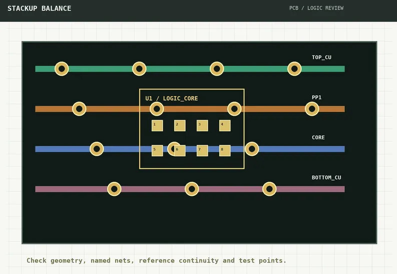
Why a PCB Still Warps When Copper Thickness Is the Same but the Stackup Is Asymmetric
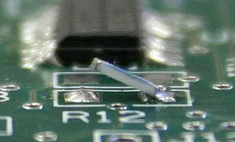
Can a Via Be Placed in a Pad? A Detail PCB Designers Cannot Skip
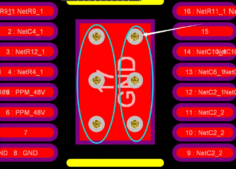
Why More Thermal Vias Do Not Always Mean a Lower PCB Temperature
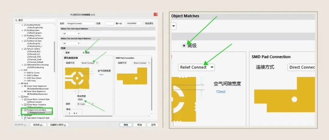
Why Does a Pad Tied Straight to a Copper Pour Become More Prone to Poor Soldering?

What Is the Purpose of a Via in a PCB?

PCB Material and Thermal Design Requirements for Reliable Assembly

Clock Circuit Layout and Routing for Crystals and Oscillators

PCB Routing Safety: Trace Width, Clearance, and Thermal Rules

Why Do PCBs Use Thermal Relief Pads?
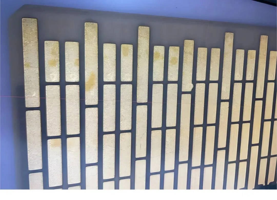
Why Do Optical Modules Use Segmented Gold Fingers?
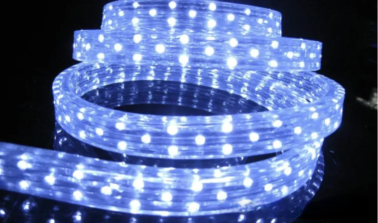
Why LEDs Emit Light but Ordinary Diodes Do Not
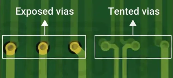
Should a PCB Via Be Tented or Exposed? Do Not Select the Wrong Option by Habit
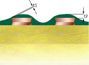
PCB Solder Mask Thickness: When It Is Too Thick, It Becomes Armor; When It Is Too Thin, It Creates Hidden Risks
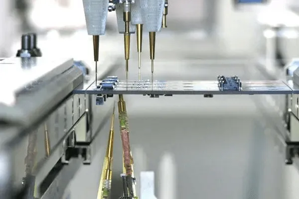
PCB Power Stability Testing
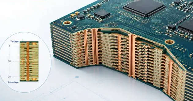
Multilayer PCB Assembly: Design and Manufacturing Considerations
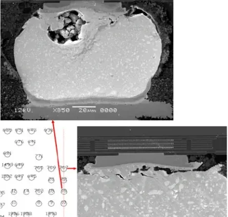
Temperature Is a Major Threat to Reliability