 00:55
00:55
HDI PCB
High Density Interconnect (HDI) PCBs represent a cornerstone of modern electronics design, enabling the creation of compact, high-performance devices that power everything from smartphones and wearables to advanced medical equipment and automotive systems. These specialized circuit boards feature finer lines, smaller vias, and multiple layers of interconnects, allowing for greater component density without sacrificing reliability or signal integrity. For engineers and designers searching for HDI PCB solutions, this tag serves as a comprehensive resource, delving into the intricacies of their construction, including microvias, buried vias, and sequential lamination techniques that facilitate miniaturization while maintaining electrical performance. Understanding HDI PCBs is essential for tackling challenges in space-constrained applications, where traditional PCBs fall short. Key advantages include reduced signal loss, improved thermal management, and enhanced functionality through higher layer counts, making them ideal for high-speed data transmission in 5G networks or intricate IoT devices. Practical insights here cover best practices such as selecting appropriate materials like high-Tg laminates for thermal stability, optimizing via structures to minimize impedance issues, and implementing design rules that prevent manufacturing defects. By applying these strategies, you can achieve cost-effective production and faster time-to-market, whether prototyping a new gadget or scaling up for mass production. For those seeking to deepen their knowledge, the articles linked under this tag offer detailed case studies, tutorials on CAD tools for HDI layout, and comparisons with standard PCBs to guide informed decision-making in your projects.
Video Guide
-
00:55
-
 00:45
00:45
The Fastest Way to Waste Money on Your First PCB
-
 00:57
00:57
PCB Antipad Design: 4 Key Factors for Reliable High-Speed Multilayer PCBs
-
 00:58
00:58
What Is an HDI PCB? High Density Interconnect Explained
-
 01:01
01:01
HDI PCB Fundamentals: Microvias, Density, and High-Speed Performance
-
 01:09
01:09
How Signals Jump Between PCB Layers: Vias Explained
Technical Articles
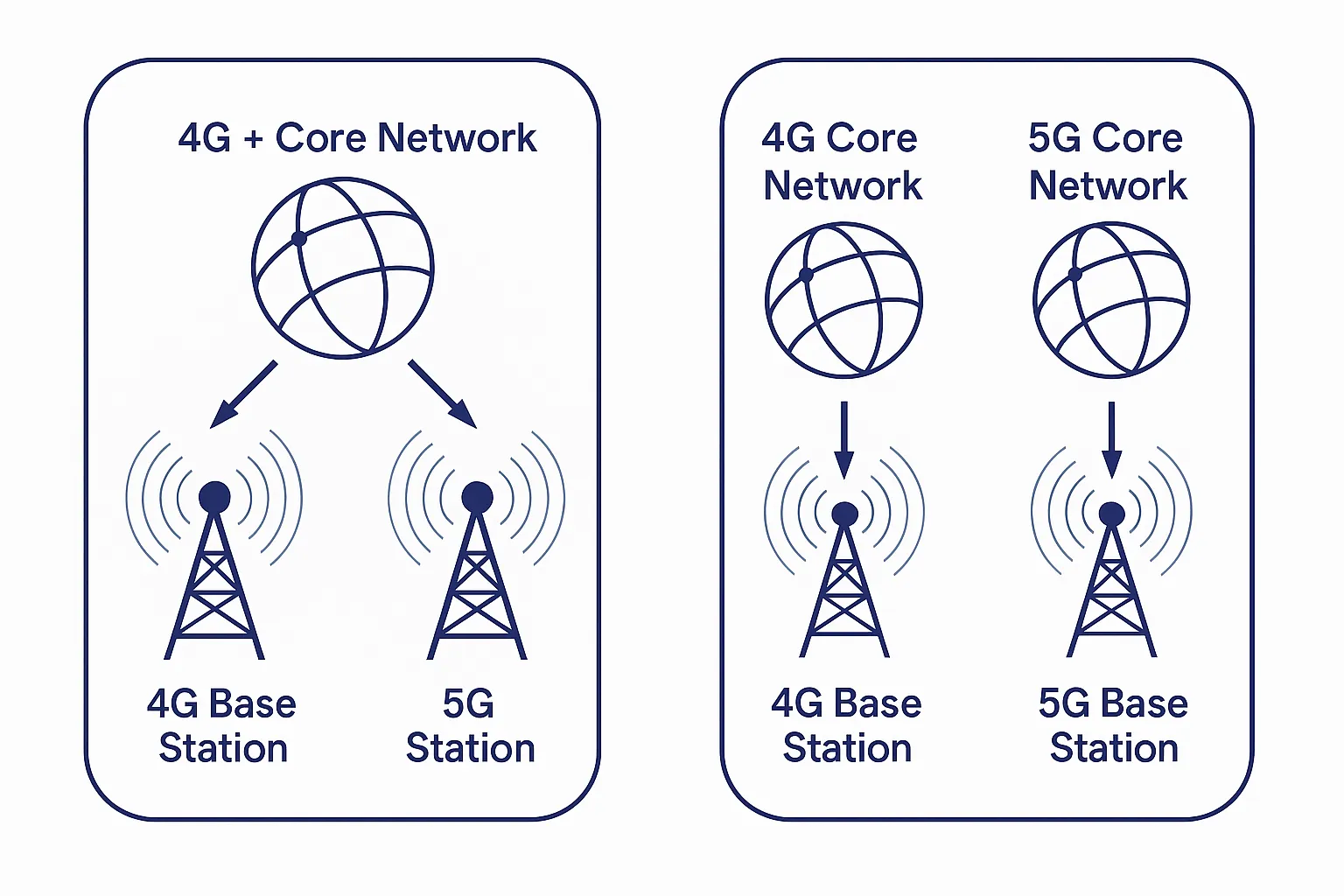
Advanced 5G Technologies: Network Slicing, RedCap, VoNR, and PCB Design Requirements for High-Performance Implementation
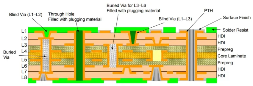
Miniaturized HDI PCB: Design and Manufacturing for Small Form Factor Electronics
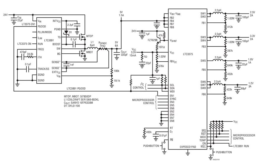
Multi-Output Buck Converter Design with LTC3375: Power Management for Industrial PCB Systems
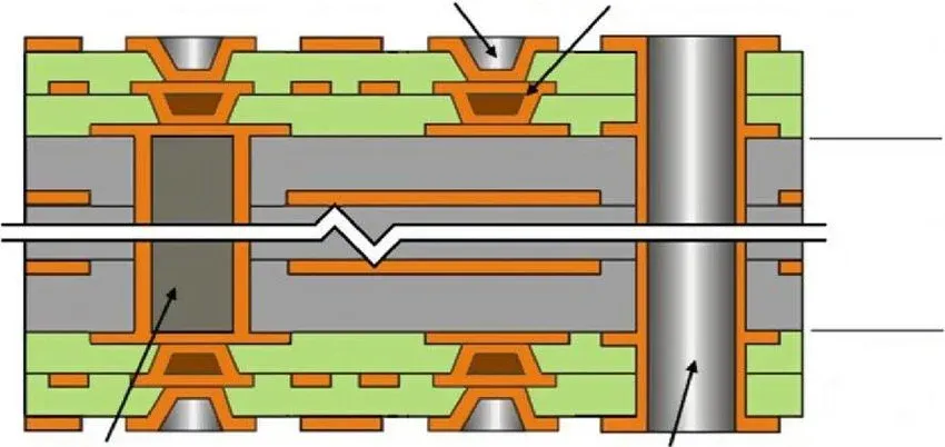
Advanced HDI PCB: Materials, Manufacturing, Design, and Interconnect Technology
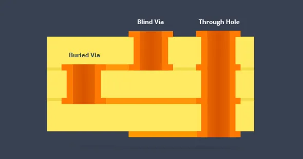
Via Technology in PCB Manufacturing: Types, Design Rules, and Optimization Techniques
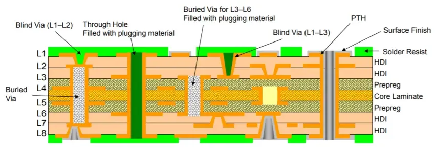
HDI Stacked Via PCB Design Rules: Best Practices for Optimal Performance
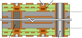
The Ultimate Guide to Stacked Via Aspect Ratio: Balancing Performance and Manufacturability
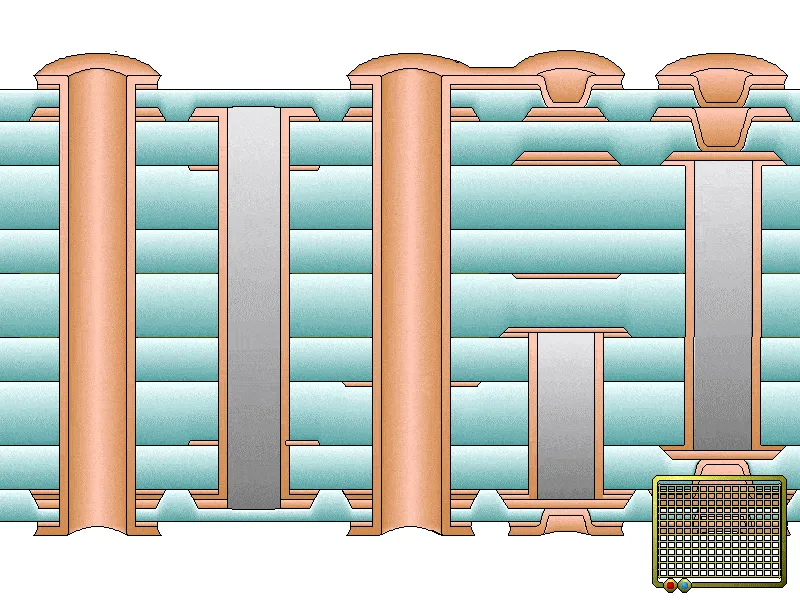
Stacked Via PCBs in Medical Devices: Ensuring Performance and Safety
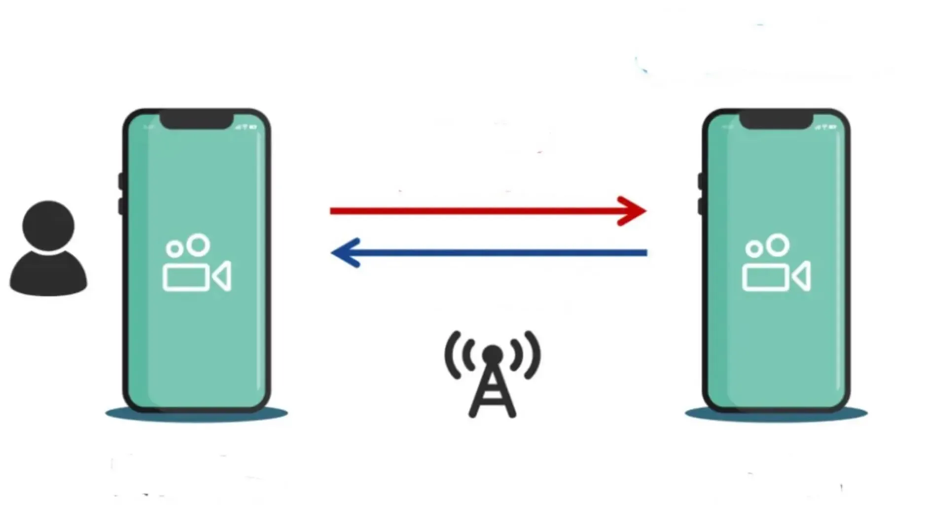
What Is a Cloud Phone? Architecture, Applications, and Electronics Requirements
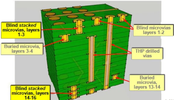
Troubleshooting Stacked Via Problems: A Practical Guide
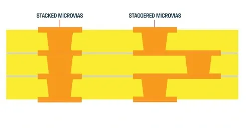
Stacked Vias vs. Staggered Vias: Choosing the Right Via for Your PCB Project
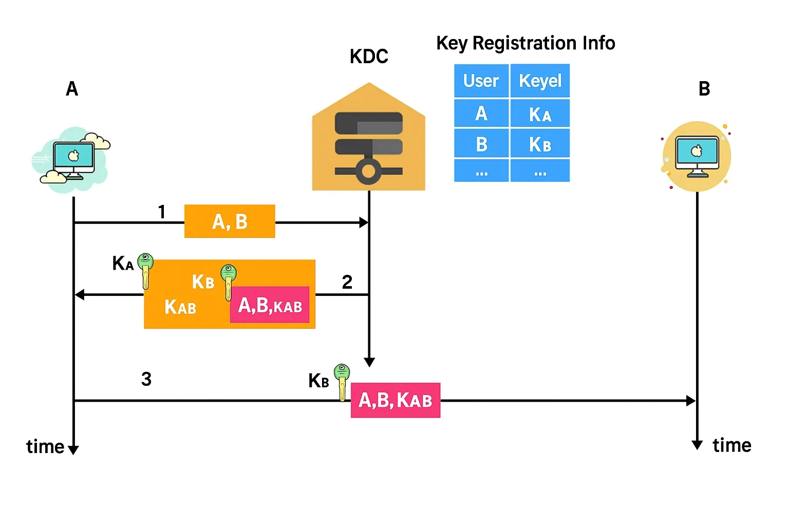
PCB Design and Manufacturing Considerations for Enterprise Firewalls, Network Security Systems, and NAT Traversal Solutions
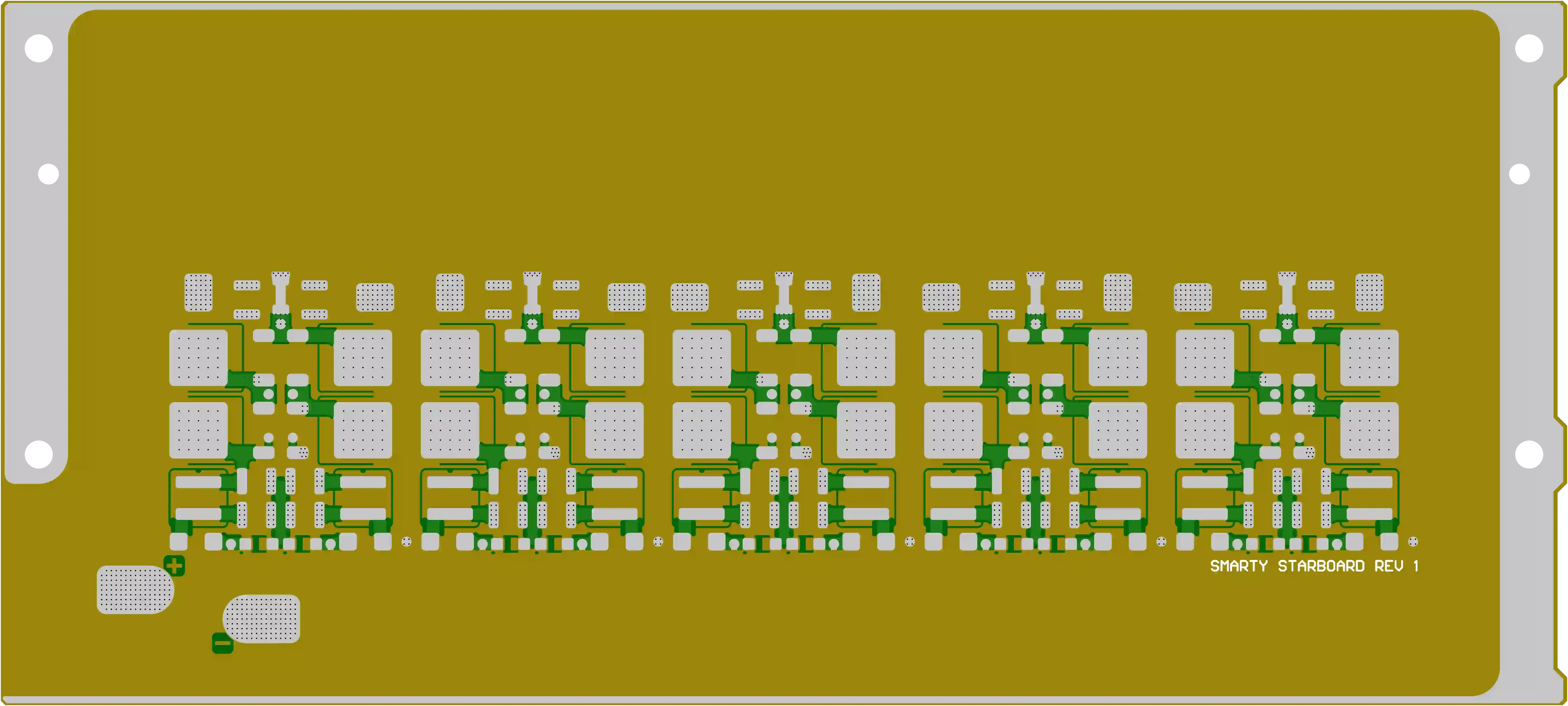
0.15mm Hole & Countersink Depth Control in 4-Layer HDI PCB
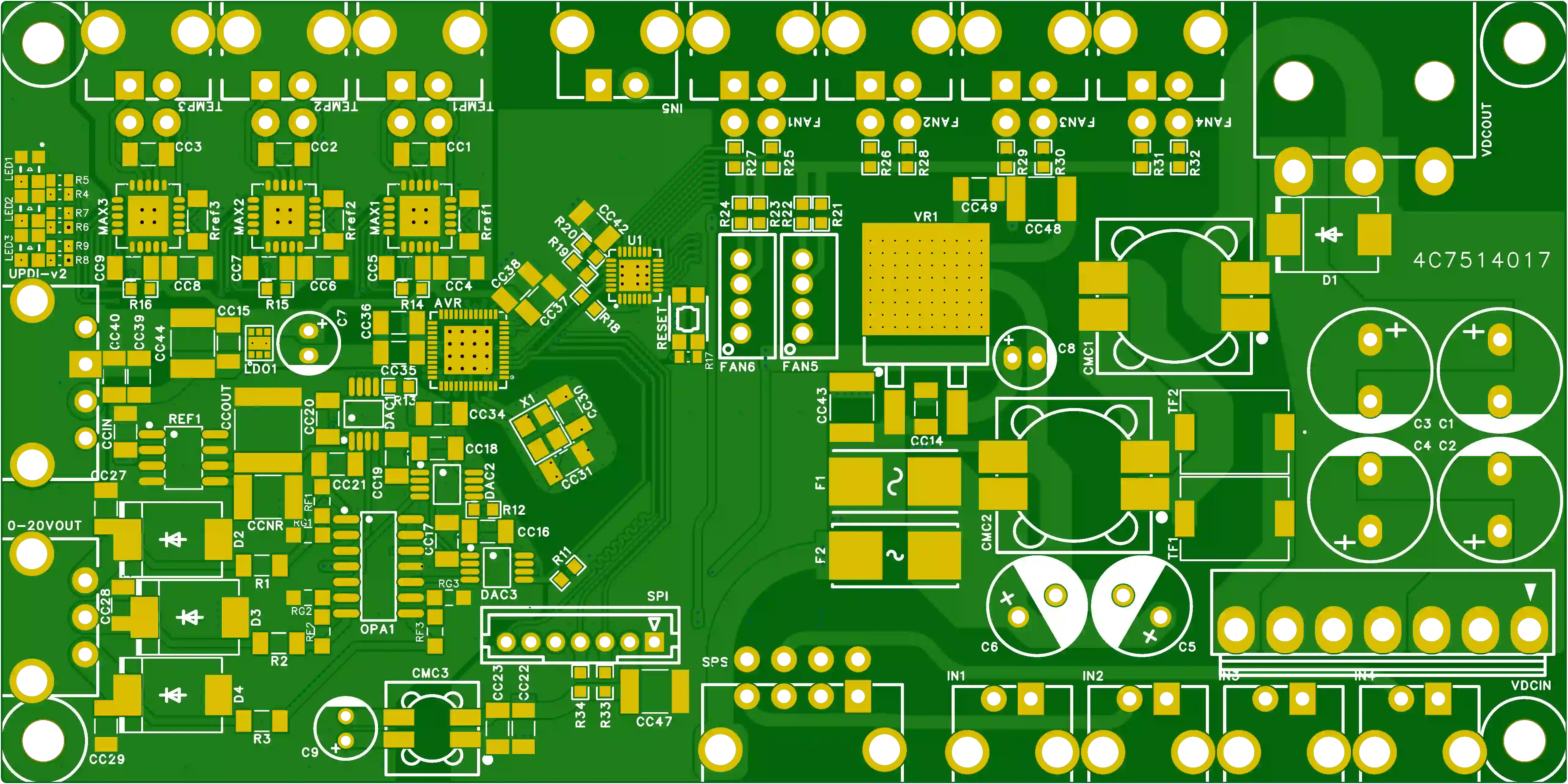
How Conflicting Via Data and Soldermask Definitions Triggered CAM Review in a 4-Layer HDI PCB
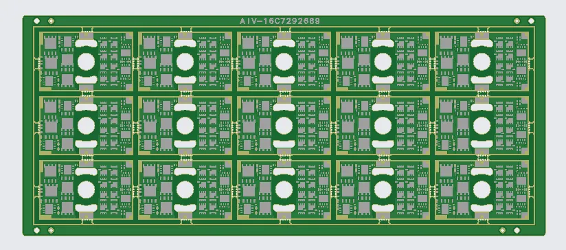
16 Layer PCB CAM Review: HDI Stackup Optimization and Resin Plugging for Reliable Fabrication
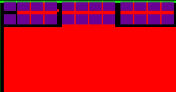
How PCB CAM Review Resolves Copper Weight and Panelization EQs on 8-Layer HDI Boards

4-Layer HDI PCB Engineering Review Case: Stackup Deviation, Countersink Hole Depth, and Material Availability Challenges
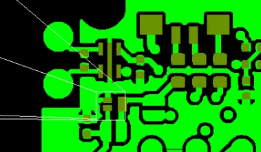
Resin Filled Via & Blind Via Issues in 6-Layer 2nd Order HDI PCB CAM Review

Building Insights from a Polaroid Photo Frame Hack – PCB Reverse Engineering Journey