High-Speed PCB
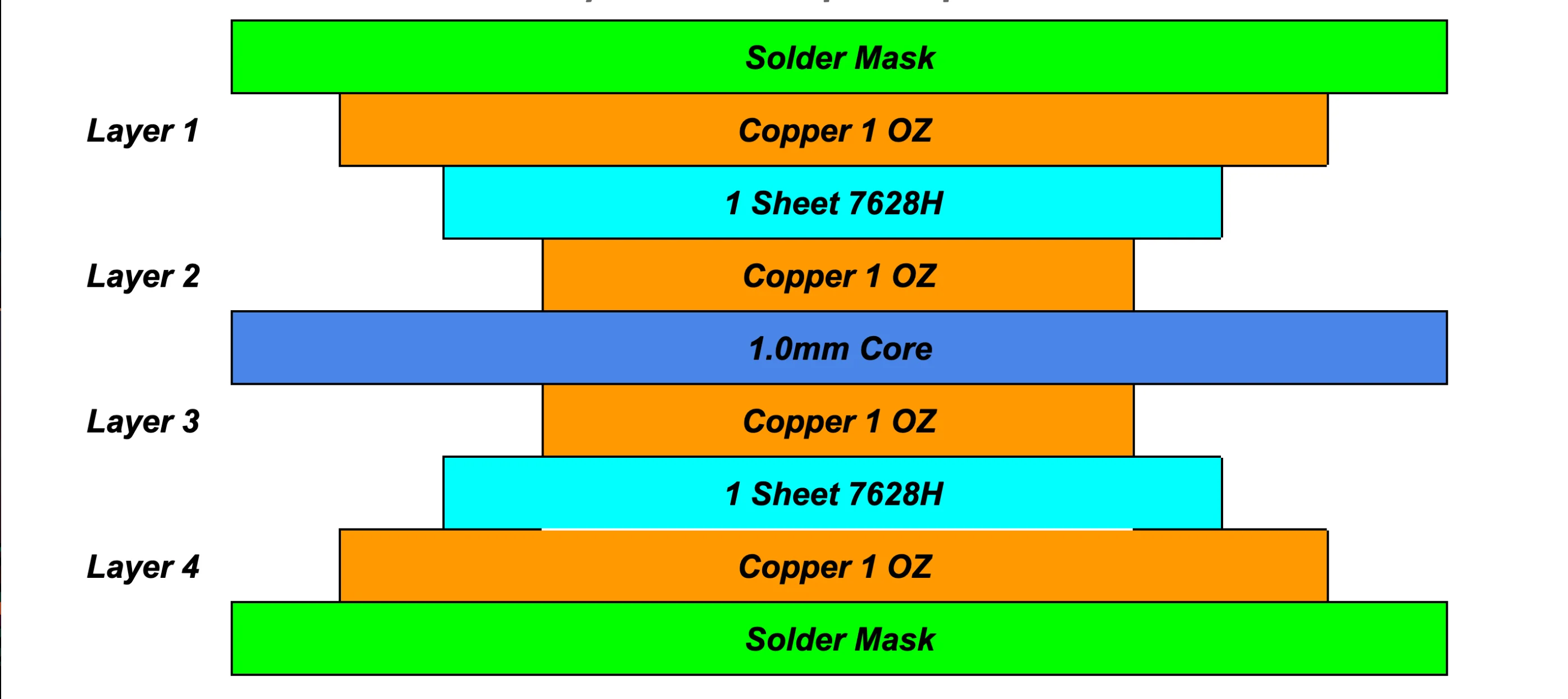
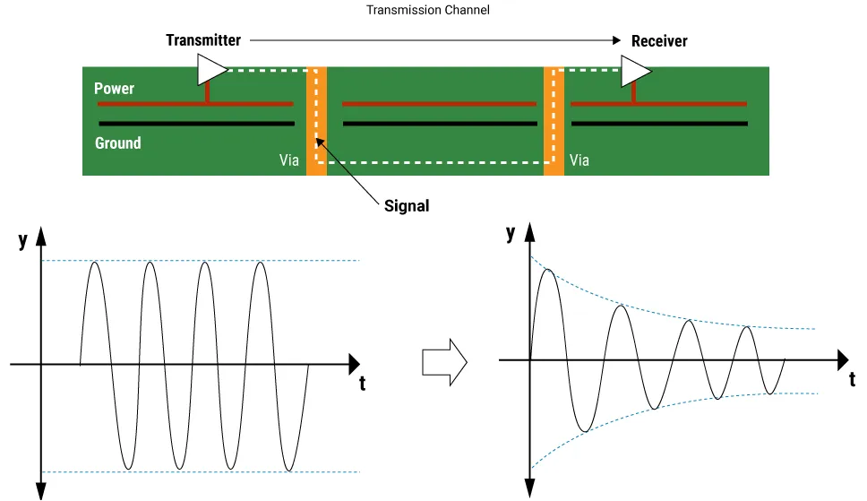
High-speed printed circuit boards (PCBs) are essential components in modern electronics, enabling the reliable transmission of signals at frequencies exceeding 100 MHz. These specialized boards address the challenges of signal integrity, electromagnetic interference, and thermal management in applications such as telecommunications, data centers, automotive systems, and high-performance computing. For engineers and designers searching for High-Speed PCB resources, this tag serves as a comprehensive hub, offering in-depth guidance on optimizing designs to prevent issues like crosstalk, reflections, and timing errors that can degrade performance. Understanding the fundamentals of high-speed PCB design begins with selecting appropriate materials, such as low-loss dielectrics and controlled-impedance traces, to maintain signal quality over long distances. Best practices include implementing proper layer stacking for multilayer boards, using differential signaling to reduce noise, and incorporating ground planes to minimize EMI. Practical applications often involve simulation tools like SPICE or electromagnetic field solvers to predict and mitigate potential problems before prototyping, saving time and costs in the development cycle. For instance, in 5G infrastructure, high-speed PCBs ensure seamless data transfer rates, while in consumer electronics, they support faster processing in devices like smartphones and gaming consoles. Professionals tackling high-speed projects can benefit from actionable insights on via optimization, such as back-drilling to eliminate stubs, and routing techniques that prioritize signal path length matching. This collection of articles explores these topics through real-world examples and case studies, helping you apply proven strategies to your own designs. Whether you are refining an existing layout or starting a new high-frequency project, the resources here provide the technical depth needed to achieve robust, efficient results.
Technical Articles
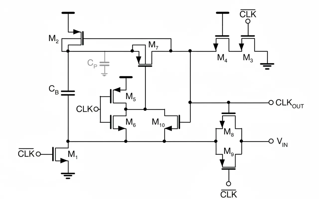
Two Sources of Sampling-Switch Error in ADCs
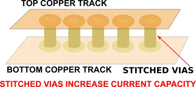
Via Stitching: Your Secret Weapon for Reducing EMI in PCBs
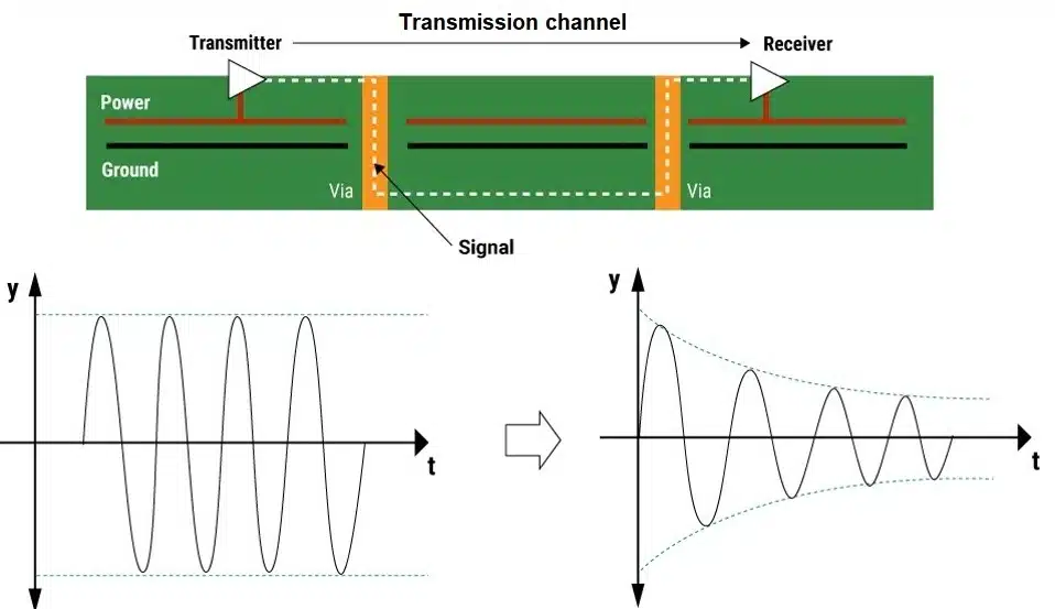
Jitter Free PCBs: A Practical Guide to Layout and Design
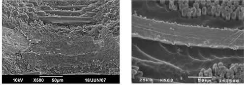
Advanced PCB Etch Back Techniques Using Plasma: Improving Interlayer Connections
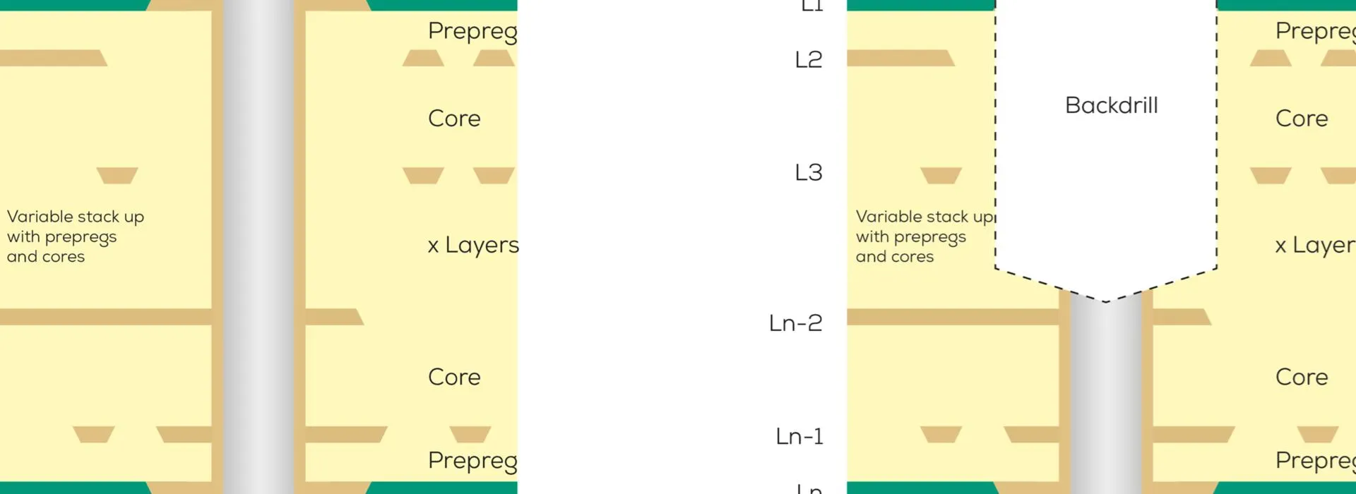
The Impact of Controlled Depth Drilling on High Speed PCB Performance
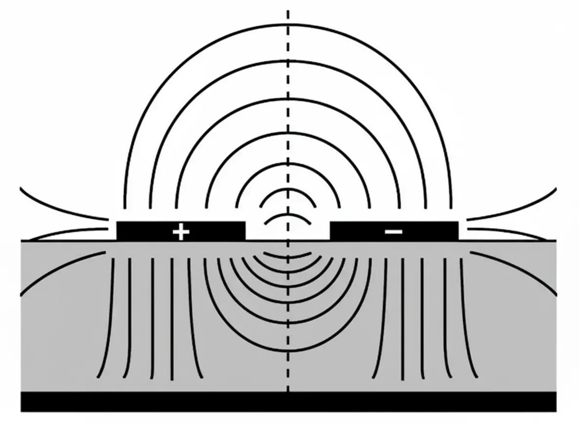
Differential Signal Return Paths in PCB Design: Analysis & Best Practices
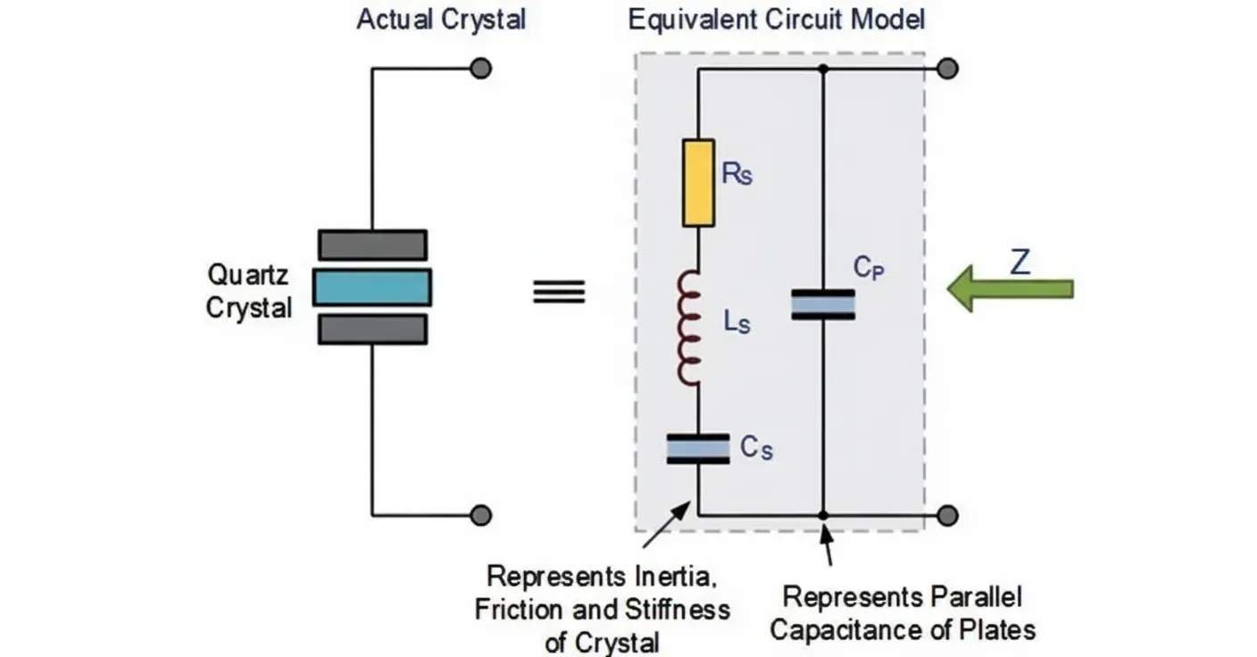
Quartz Crystals and Oscillators: Fundamentals, PCB Design, and Manufacturing Considerations
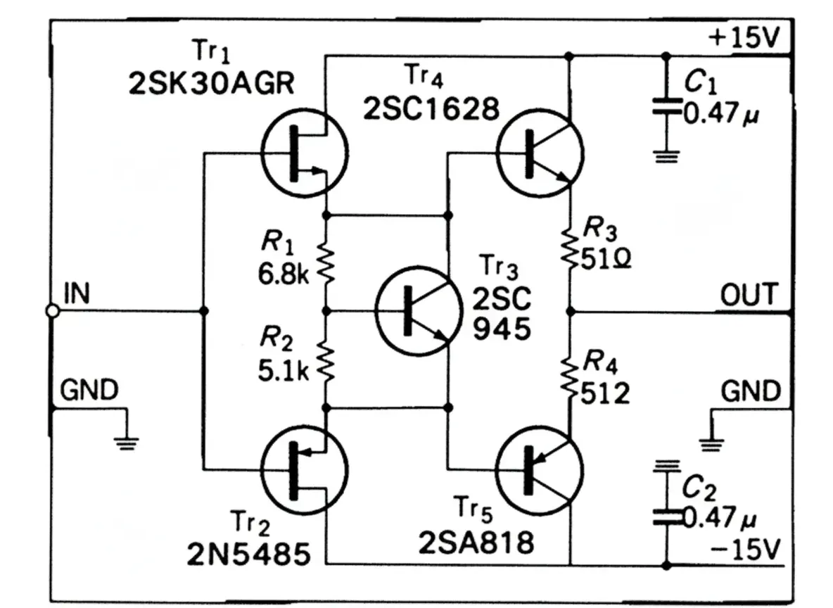
Push-Pull Buffer Amplifier Using Complementary FETs
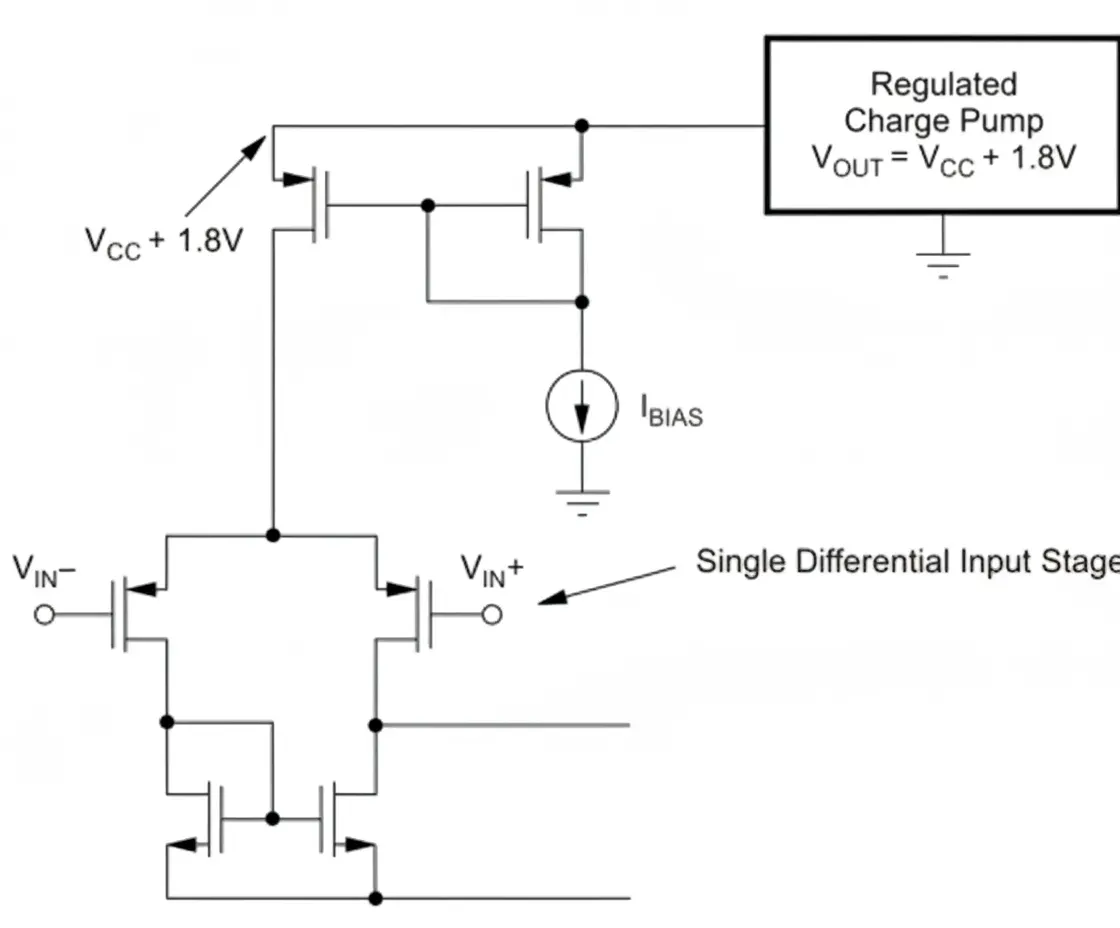
Single-Supply Op Amp Designs for Rail-to-Rail Input
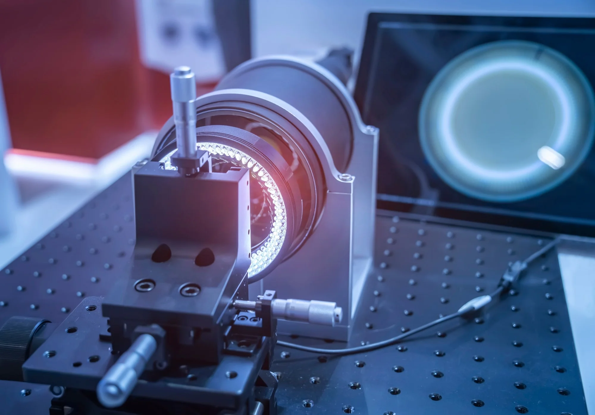
Optoelectronic Sensor Technology: Principles, Applications, and PCB Integration
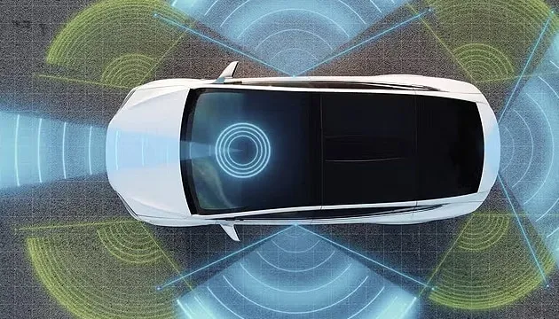
LiDAR vs Vision: Comparing ADAS Routes
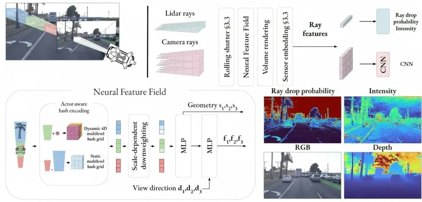
NeuRAD: NeRF for Dynamic Autonomous Driving Data
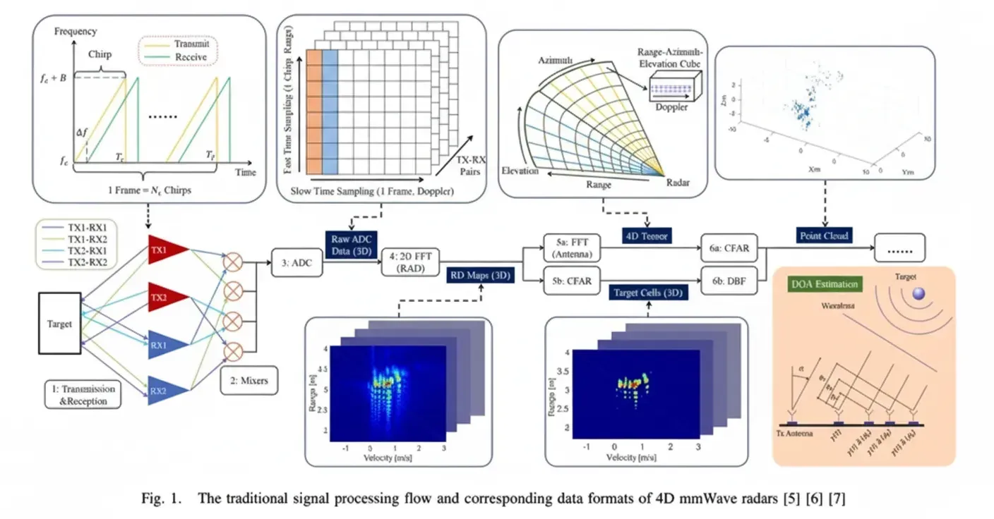
Survey of 4D Millimeter-Wave Radar SLAM Approaches
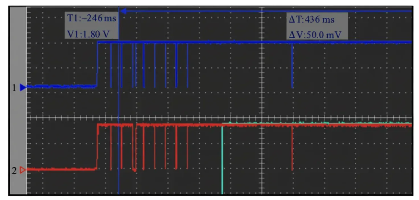
Effect of Noise Sources on Infrared Sensor Performance

Sensor Roadmap for the Next Decade
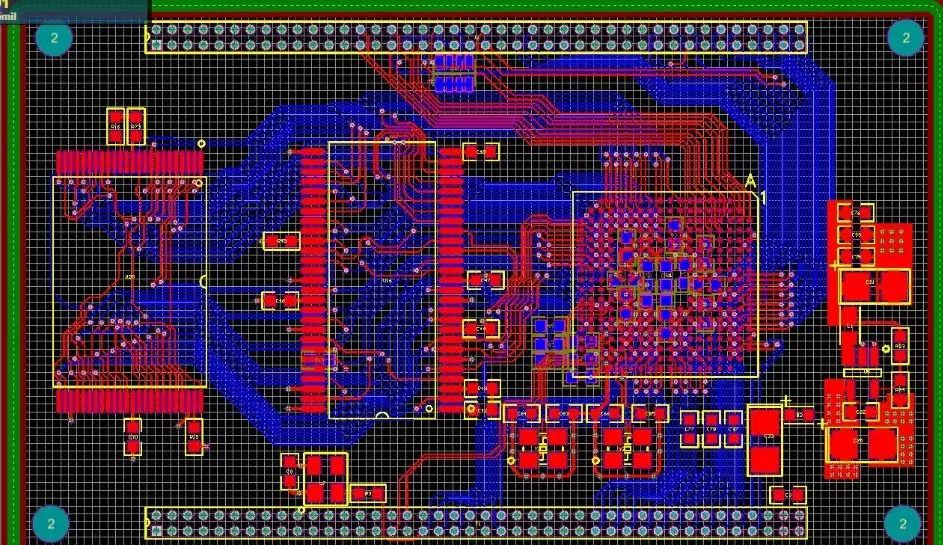
The Ultimate Guide to Minimizing Jitter in Your PCB Layout
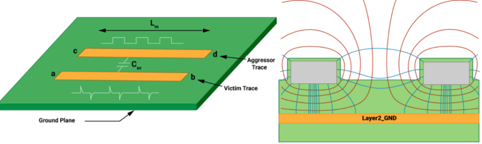
Mastering PCB Layout: Jitter Control Techniques for High Speed Signals
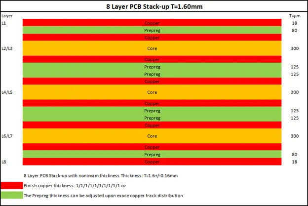
8 Layer PCB Stack Up: Advanced Design Techniques for High Speed Circuits