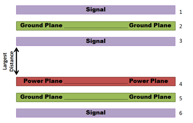
Mixed-Signal Grounding
Mixed-signal grounding refers to the specialized techniques used in printed circuit board (PCB) design to manage ground planes in systems that integrate both analog and digital components. This approach is essential for minimizing noise interference, ensuring signal integrity, and preventing issues like ground loops that can degrade performance in sensitive electronics. Engineers and designers often search for information on mixed-signal grounding when troubleshooting problems such as electromagnetic interference (EMI) or when optimizing layouts for applications like audio equipment, sensors, or communication devices. By separating analog and digital grounds while providing a common reference point, typically through a star grounding scheme or careful partitioning, you can achieve cleaner signals and more reliable operation. Understanding the principles of mixed-signal grounding empowers you to apply best practices in real-world scenarios. For instance, placing analog components away from high-speed digital traces and using ferrite beads or decoupling capacitors can significantly reduce crosstalk. In high-frequency designs, techniques like multi-layer PCBs with dedicated ground planes become crucial to isolate noise sources. These methods not only comply with standards such as those from the IPC but also enhance overall system efficiency, making them invaluable for hobbyists building prototypes or professionals developing commercial products. Common pitfalls, such as improper via placement or inadequate shielding, are addressed in depth to help you avoid costly revisions. The articles under the Mixed-Signal Grounding tag delve into these topics with detailed examples, case studies, and step-by-step guides. Whether you are refining a mixed-signal PCB layout or seeking solutions to persistent noise issues, these resources provide the technical depth needed to implement effective grounding strategies in your projects.
Technical Articles
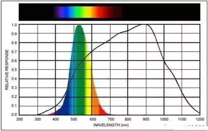
Ambient Light Sensors: Principles, Electrical Specs, and PCB Integration for Electronics Design

What Is NFC and Common NFC Applications

Short Range Wireless PCB Design for Bluetooth WiFi and Zigbee
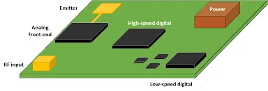
PCB RF Antenna Design and Layout: Engineering Principles, Isolation Techniques, and Manufacturing Integration
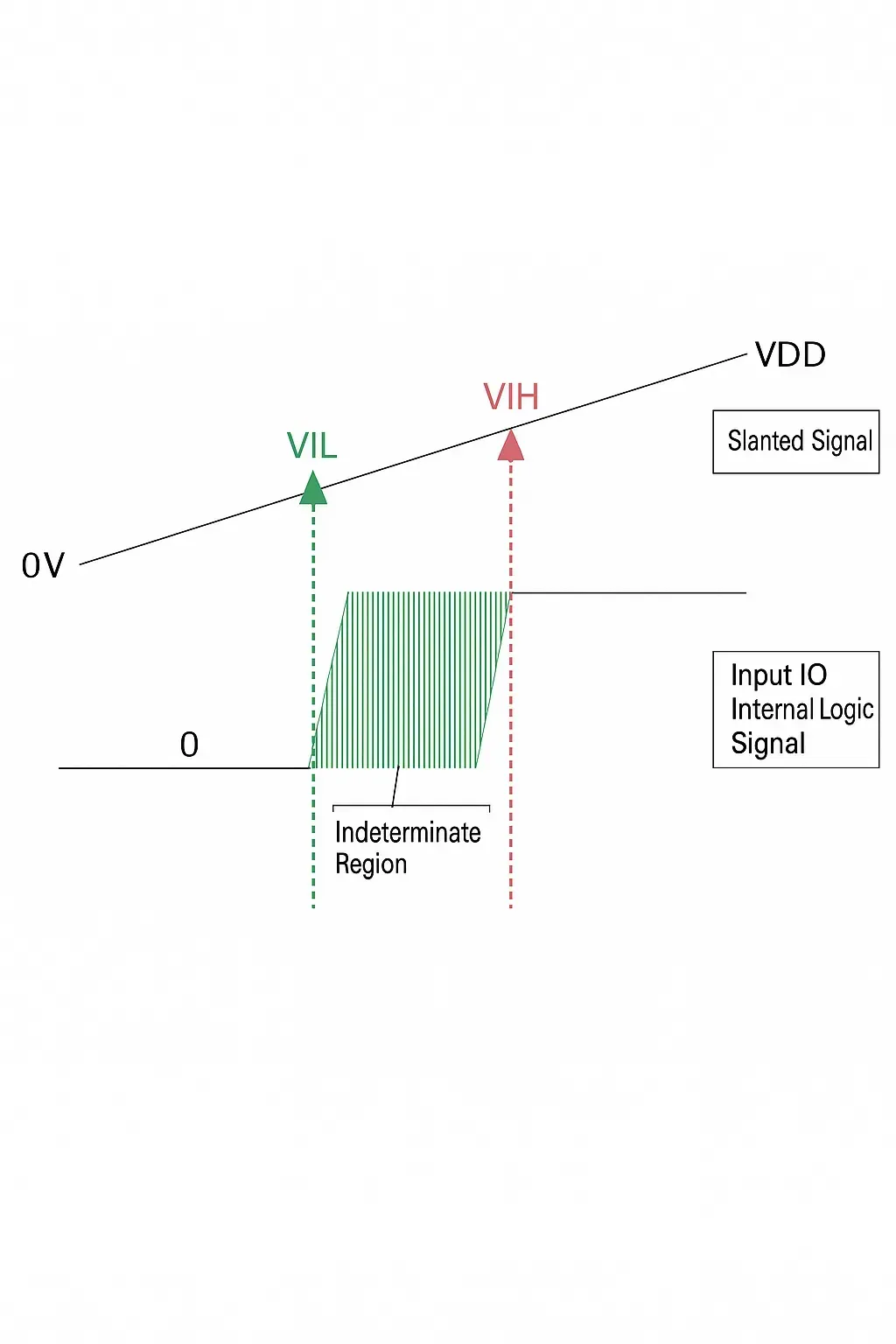
Chip IO Circuits: Design Principles, Classifications & Ground Bounce Challenges
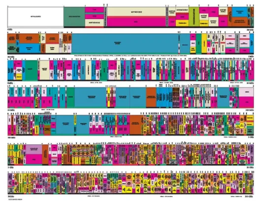
Common RF Metrics and Their Meanings
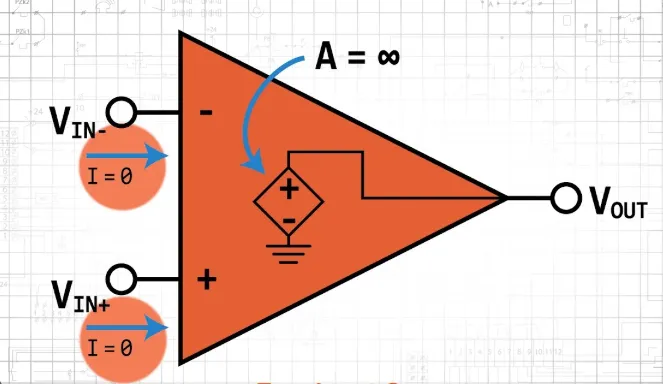
Common Op Amp Circuit Properties
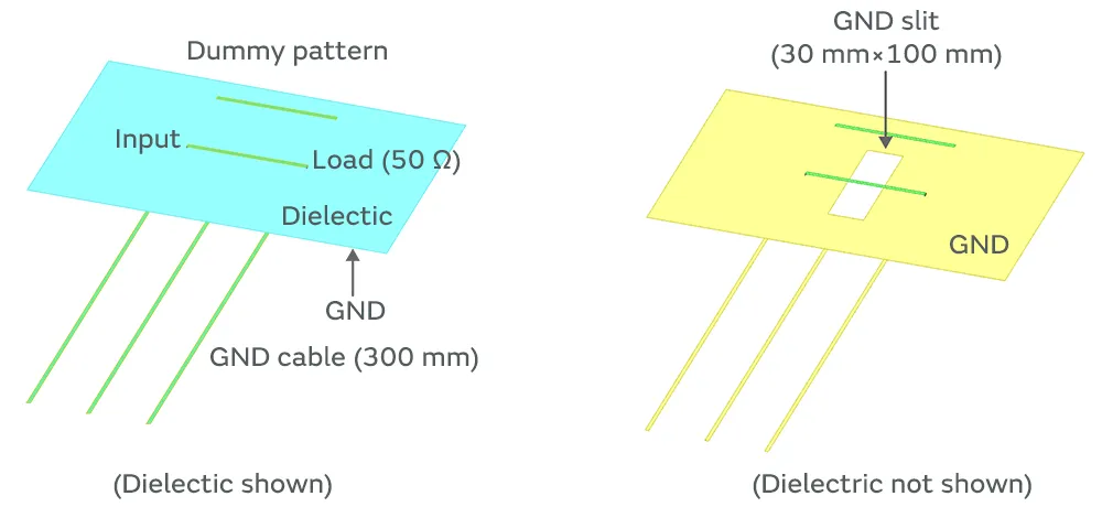
Optimizing Single Sided PCB Layout for Minimal Noise

Electronic Nose Systems: Gas Sensor Technologies, System Design, and PCB Manufacturing Considerations
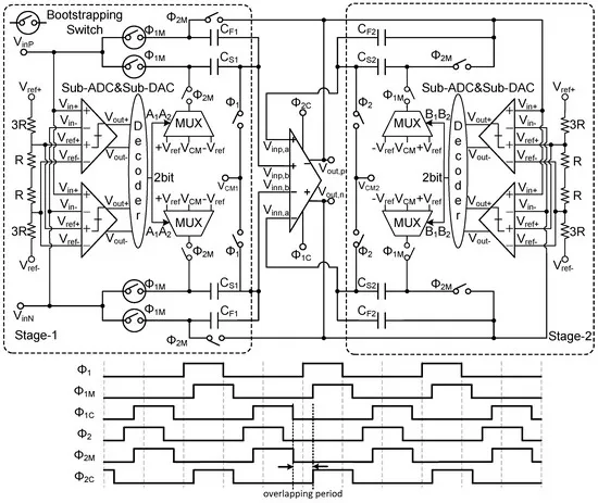
Analysis of SHA-less Pipelined ADC Architecture
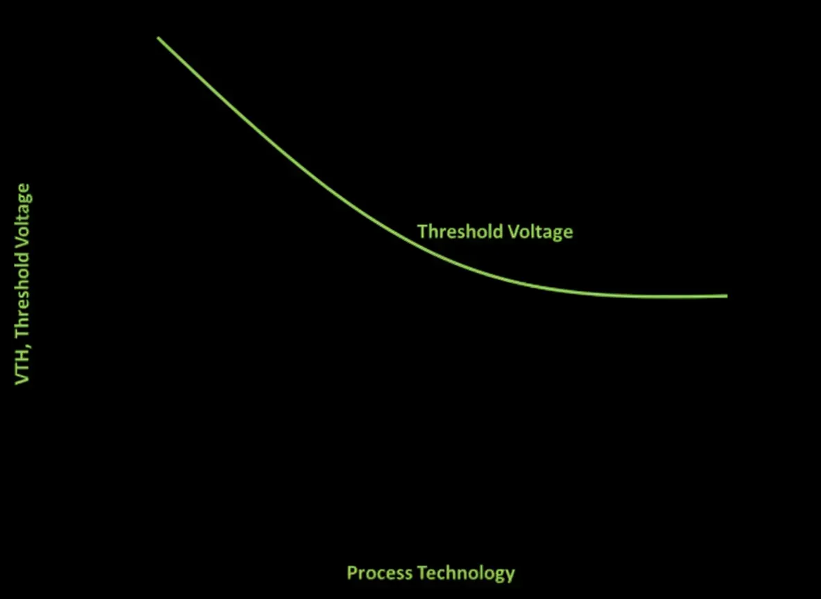
Analog-Driven SoC Design Choices in Sub-7nm Processes: Challenges & Strategies
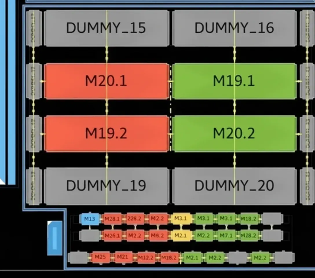
Automated Layout Techniques for Analog ICs: Differential Pairs, Common-Centroid & EDA Tools
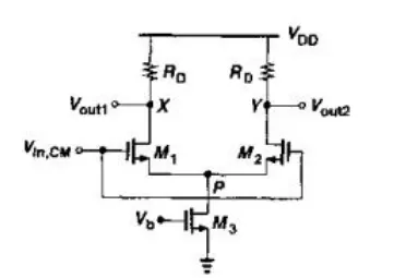
Differential Amplifier Advantages vs Single-Ended: Noise Rejection and PCB Design Insights
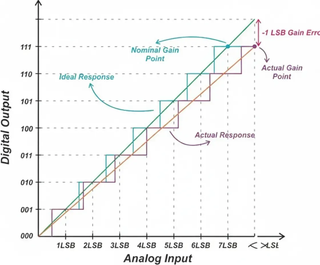
ADC Offset and Gain Error Specifications
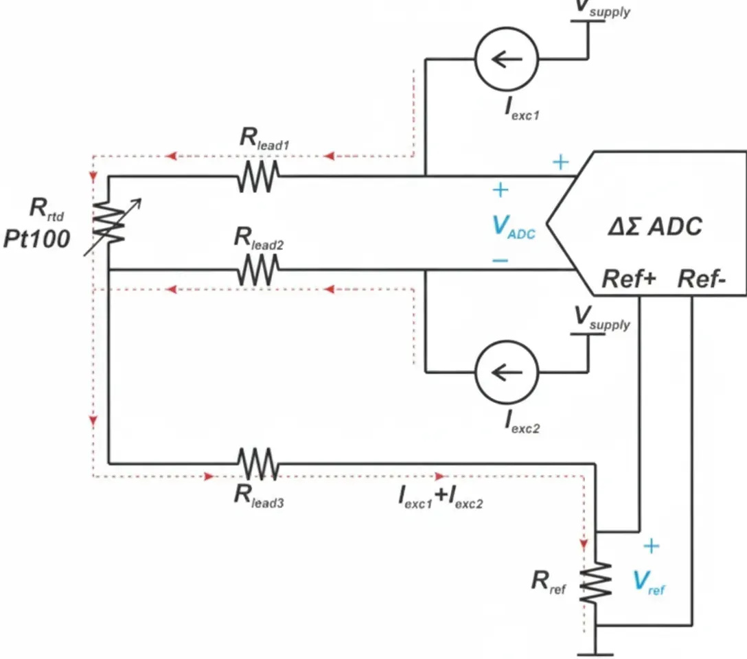
Self-Calibration and Internal Calibration in Precision ADCs
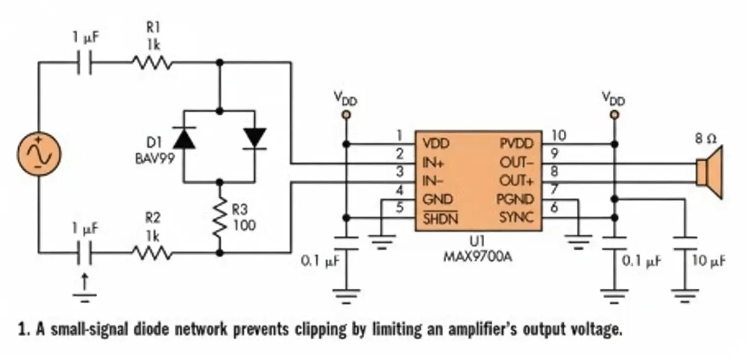
Analysis of Modified Audio Amplifier for Limiting Large Signals
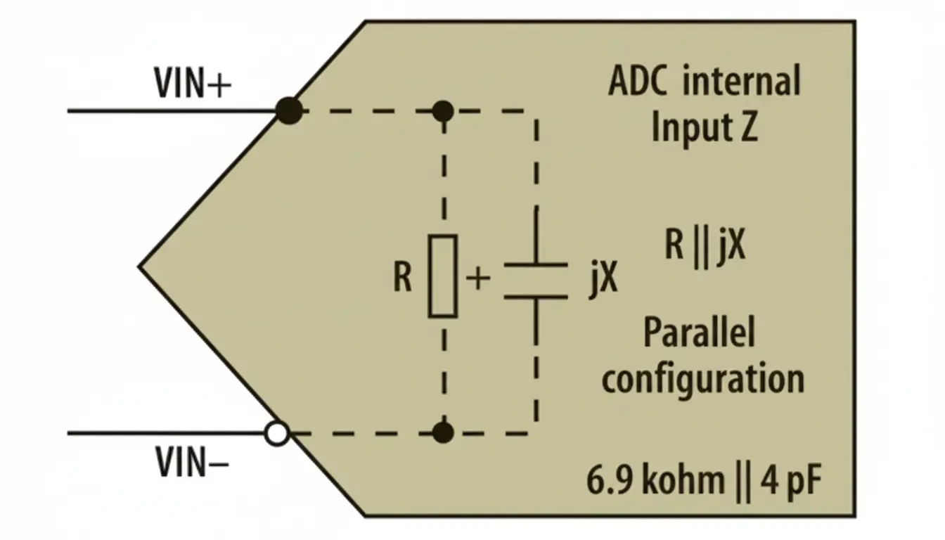
Five Practical Steps to Design an ADC Front-End
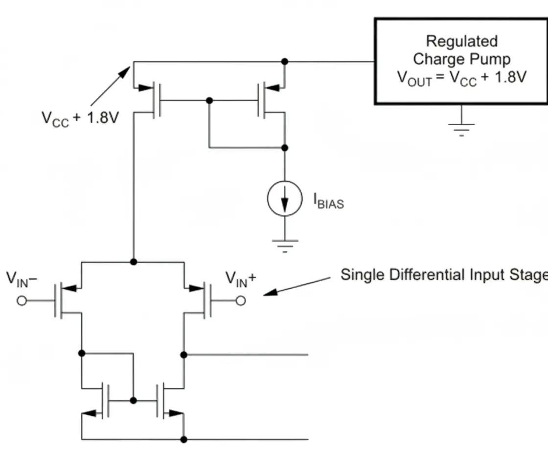
Single-Supply Op Amp Designs for Rail-to-Rail Input