 00:56
00:56
PCB Depanelization
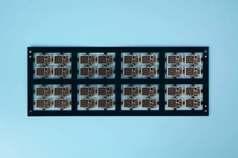
PCB depanelization is a critical step in the manufacturing process of printed circuit boards, where individual PCBs are separated from a larger production panel to prepare them for assembly and final use. This technique ensures that multiple boards produced in a single panel can be efficiently divided without compromising their integrity, functionality, or quality. For engineers, manufacturers, and hobbyists searching for information on PCB depanelization, this tag serves as a comprehensive resource, covering everything from basic concepts to advanced methodologies tailored to high-volume production or prototyping needs. Understanding the various methods of PCB depanelization is essential for optimizing efficiency and minimizing defects. Common approaches include mechanical routing, which uses CNC machines for precise cuts; v-scoring, ideal for straight-line separations on rigid boards; and laser depaneling, which offers non-contact precision for flexible or densely populated PCBs. Each method has its advantages, such as reducing stress on components or improving throughput, but selecting the right one depends on factors like board material, component density, and production scale. Best practices emphasize the importance of proper fixturing to prevent warping, regular tool maintenance to ensure clean edges, and post-depaneling inspections to catch issues like micro-cracks or delamination early. By delving into the articles tagged under PCB depanelization, readers can gain actionable insights into troubleshooting common challenges, such as handling sensitive components during separation or integrating depanelization into automated assembly lines. These resources also explore innovations like automated depaneling systems that enhance precision and reduce labor costs, helping users apply proven strategies to their own projects. Whether you are refining a manufacturing workflow or designing panels for easier separation, the content here provides practical guidance to achieve reliable results and streamline electronics production.
Video Guide
-
00:56
Technical Articles
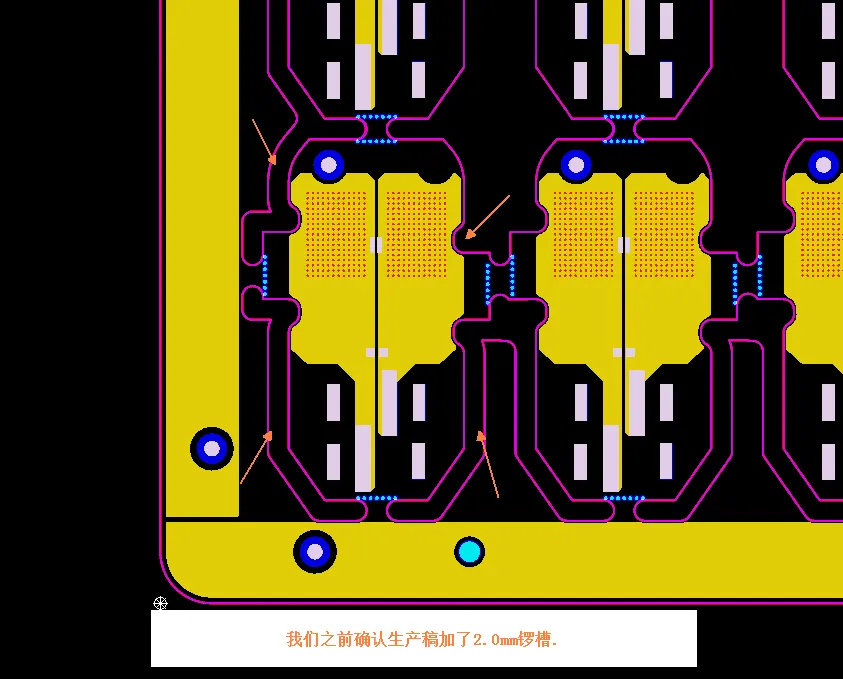
PCB Panelization Slot Design: Why Your Gerber Needs Routing Paths
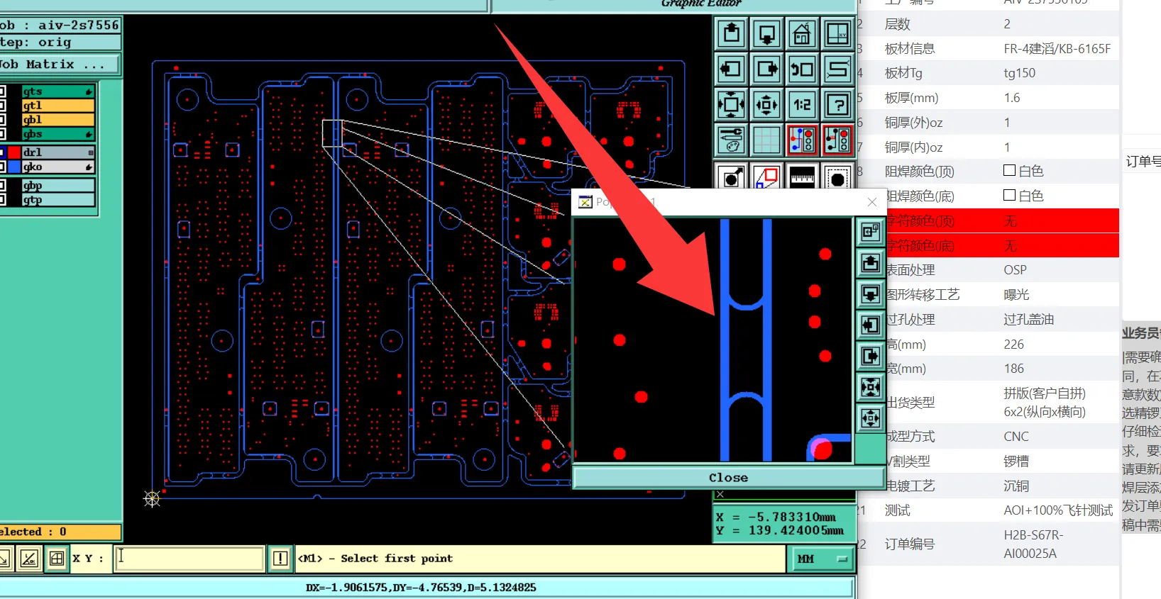
PCB Stamp Hole Design for Small 2 Layer FR4 Boards: CAM Case Study
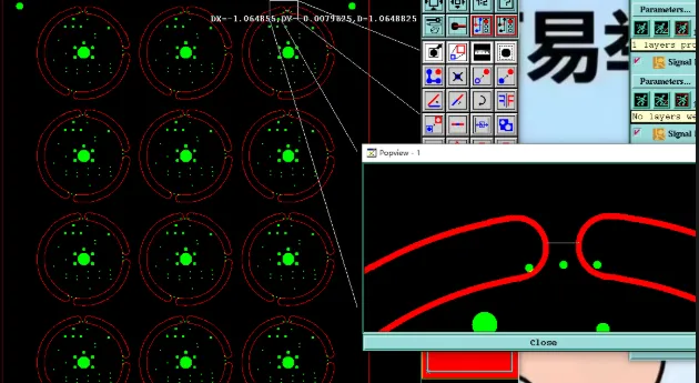
Undersized Panel Connection Tabs Risk Board Breakage in 2-Layer PCB
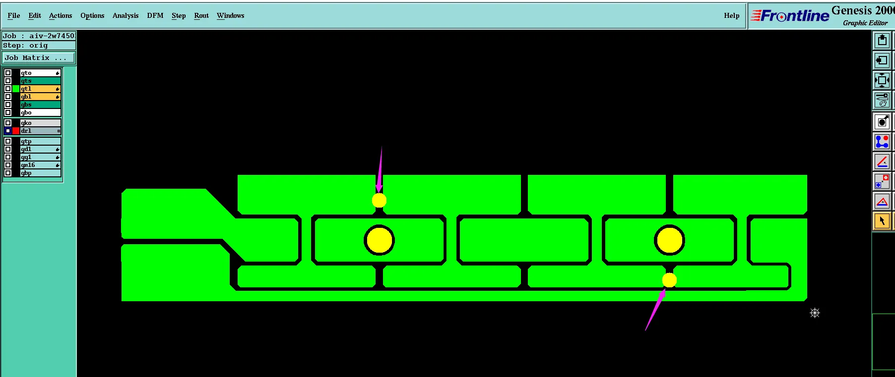
How Panelization Conflict Delayed Single Piece Delivery in 1-Layer PCB
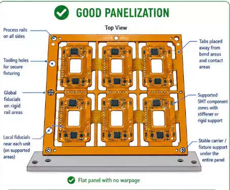
When Should You Add Waste Edge Protection on FPC Panels?
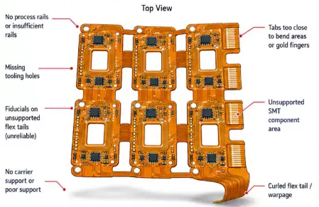
Why FPC Panels Without Process Edges on Both Ends Often Have Problems
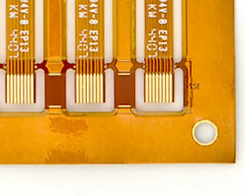
How Many Connection Points Are Needed for Stable FPC Panel Shipment?
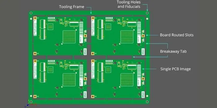
Panel Size Considerations: What is the best panel size for PCB prototype?
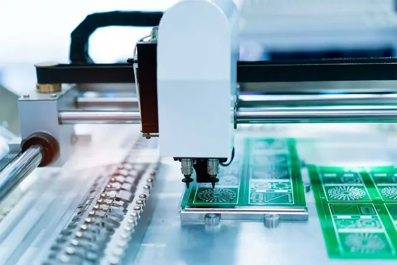
Choosing the Right PCB Depaneling Method: A Comprehensive Comparison
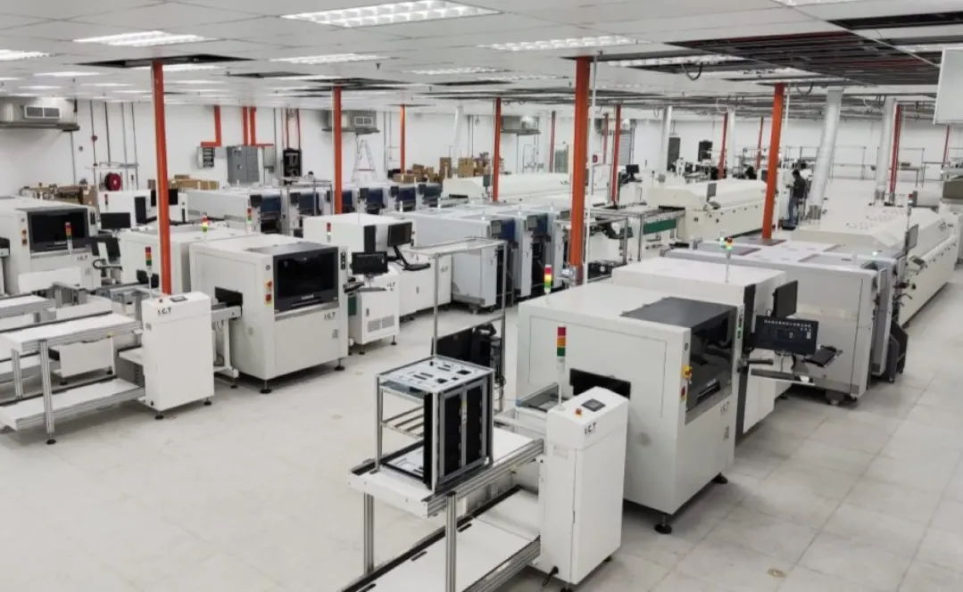
Boosting PCB Production: Integrating Depaneling Machines into SMT Lines
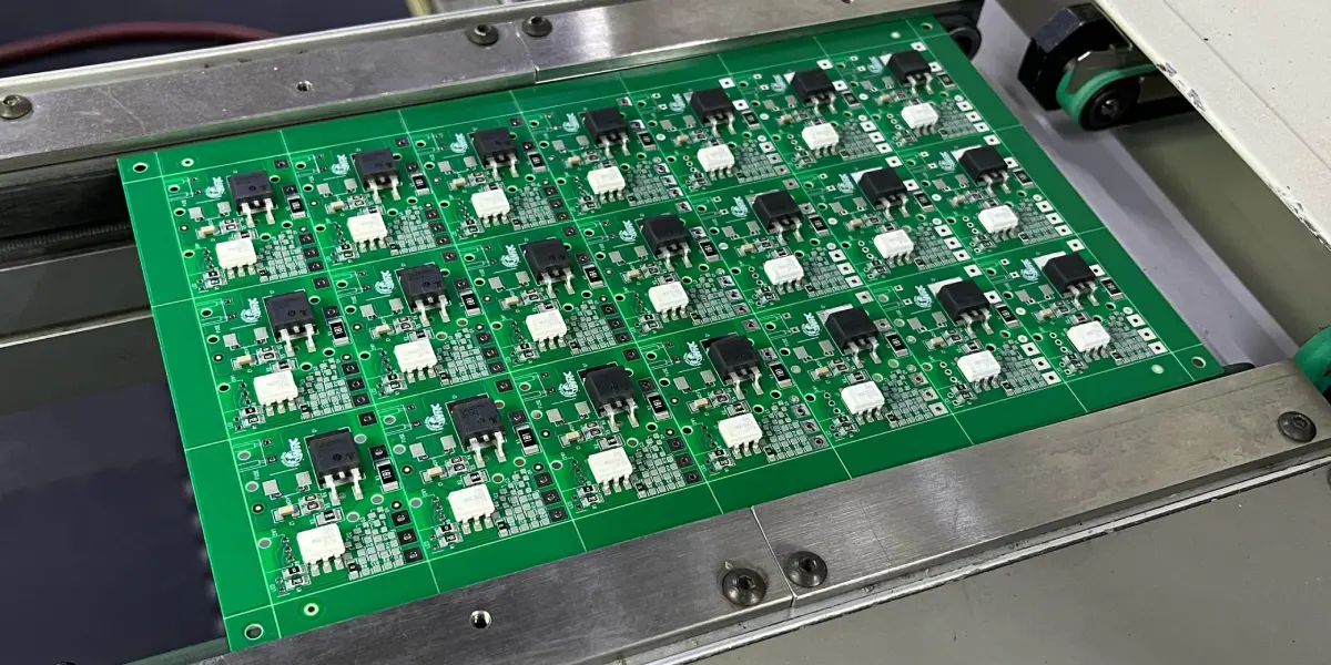
The Ultimate Guide to Depaneling Machines: Types, Features, and Applications
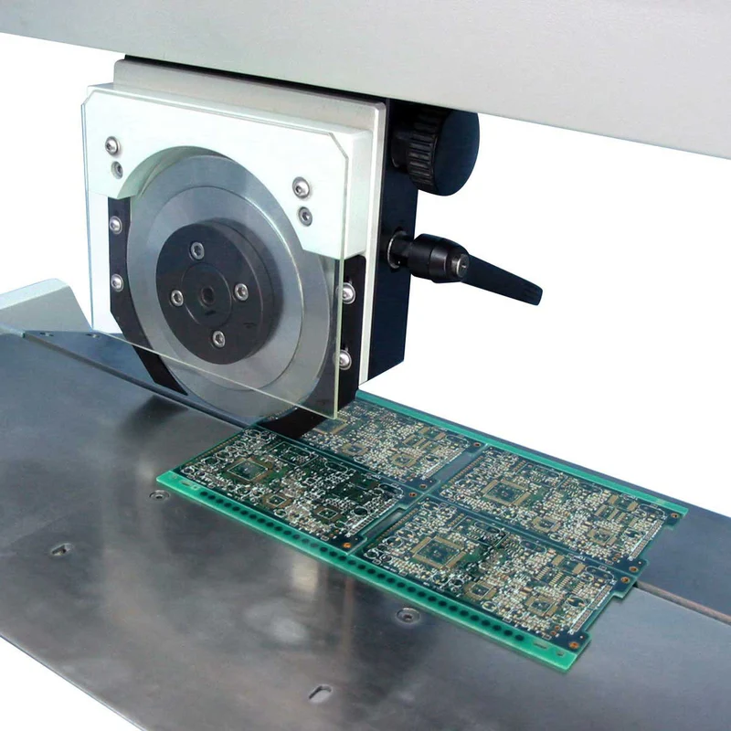
Routing vs. Laser Depaneling: Choosing the Right Machine for Your PCB Production Needs
Router Depaneling: The Go To Method for Intricate PCB Designs?
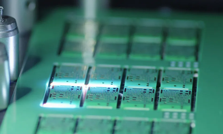
Laser PCB Depaneling: Achieving High Precision and Minimal Stress
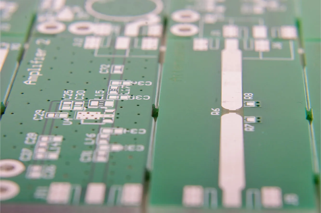
Cracking the Code: Optimizing V Scoring for PCB Depaneling Success
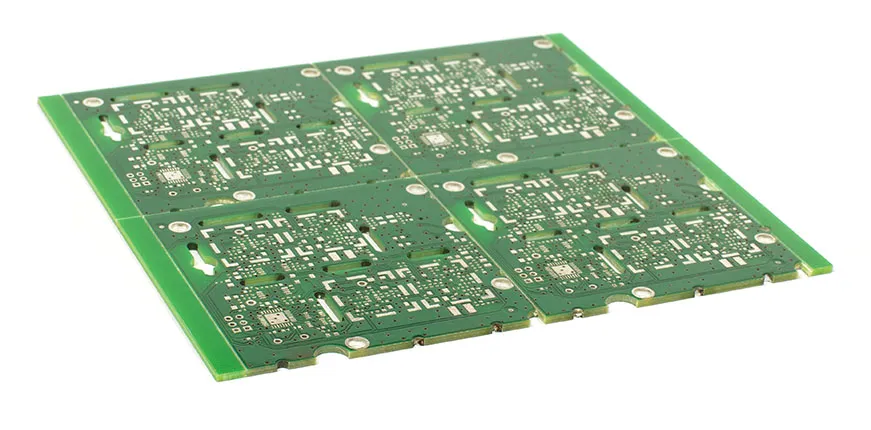
Mastering PCB Depaneling: A Step by Step Tutorial
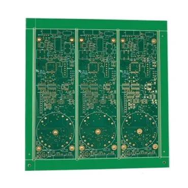
Optimizing PCB Design: V-Scoring, Component Placement, and Reliability
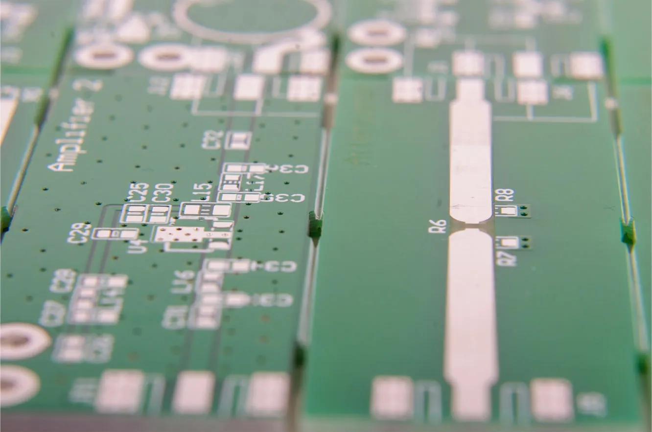
Depanelization Demystified: Mouse Bites vs. V-Score in PCB Manufacturing
V-Scoring vs. Stamp Hole: Which PCB Depaneling Method is Right for You?