Sequential Lamination
Sequential lamination is a sophisticated PCB manufacturing technique that involves building multilayer circuit boards by laminating subsets of layers in a stepwise manner, rather than pressing all layers at once. This method is particularly valuable for creating high-density interconnect (HDI) boards, where intricate via structures, such as microvias and buried vias, are essential for compact designs. By allowing precise control over layer alignment and bonding, sequential lamination minimizes issues like warping, delamination, and signal integrity problems that can plague traditional lamination processes. Engineers and designers searching for information on sequential lamination often seek ways to optimize board performance in applications like smartphones, automotive electronics, and medical devices, where space constraints and reliability are critical. One key advantage of sequential lamination lies in its ability to incorporate advanced features such as staggered vias and sequential build-up, which enhance electrical performance by reducing crosstalk and improving thermal management. For instance, in high-speed digital circuits, this technique enables finer pitch components and better impedance control, leading to more efficient signal transmission. Best practices include selecting compatible materials with matched coefficients of thermal expansion to prevent stress during multiple lamination cycles, and employing rigorous inspection methods like cross-sectional analysis to verify layer integrity. Designers should also consider the trade-offs, such as increased production time and cost, against the benefits of superior board density and functionality. For those looking to implement sequential lamination in their projects, understanding material selection and process parameters is crucial. Articles linked under this tag delve into case studies, design guidelines, and troubleshooting tips that can help refine your approach and avoid common pitfalls in PCB fabrication.
Technical Articles
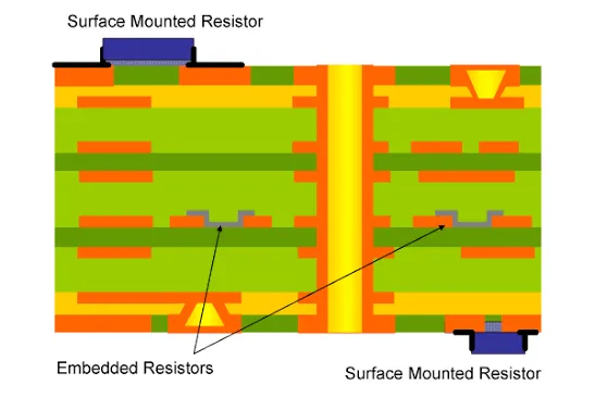
20-Layer Embedded-Resistor PCB: Process Flow and Core Manufacturing Challenges
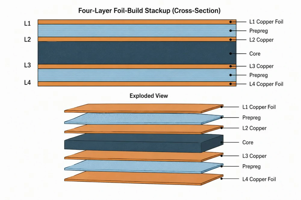
Multilayer PCB Construction Explained: Layers, Cores, Prepreg and Copper Foil

HDI Manufacturing Process Flow: From Inner Layer to Any-Layer
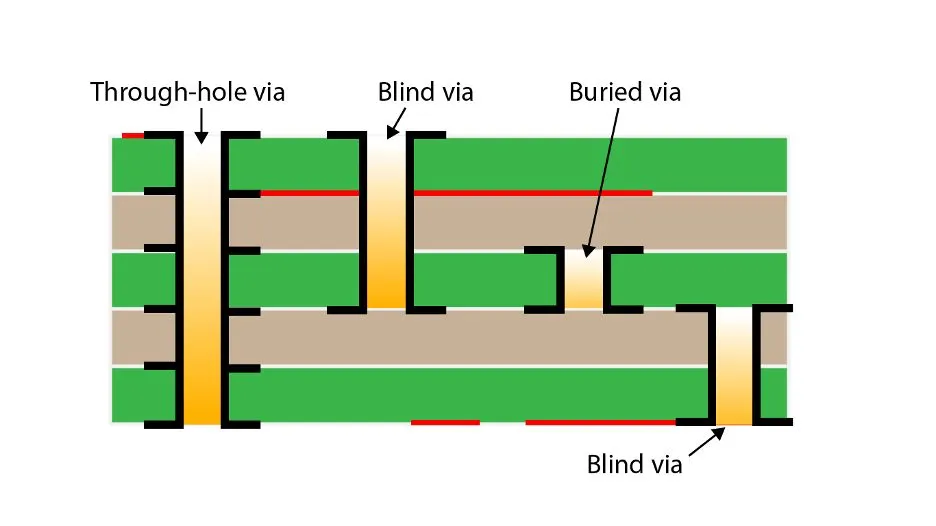
PCB Design Using Blind or Buried Vias Could Lower Fabrication Costs
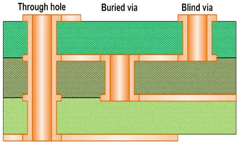
Cost Effective Buried Via Implementation: Balancing Performance and Price
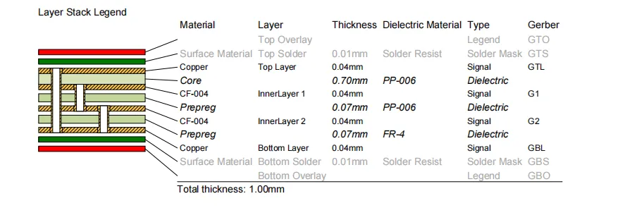
Advanced PCB Materials: Enhancing Blind and Buried Via Performance
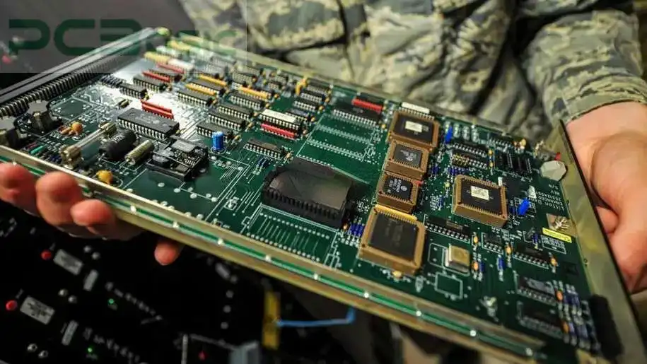
Advanced PCB Manufacturing Techniques for Military Communication Systems
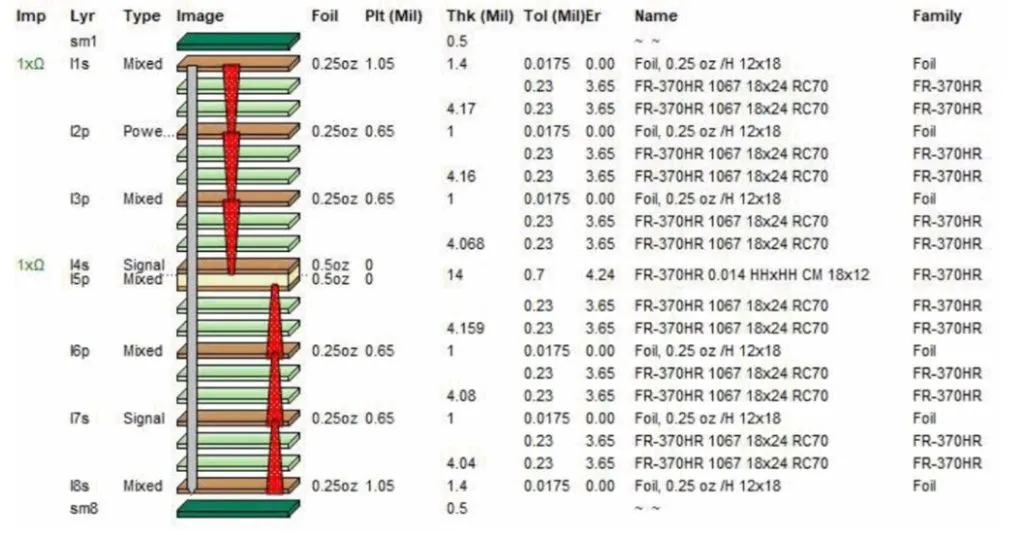
Blind and Buried Vias in Sequential Build Up PCBs: Design and Fabrication Techniques
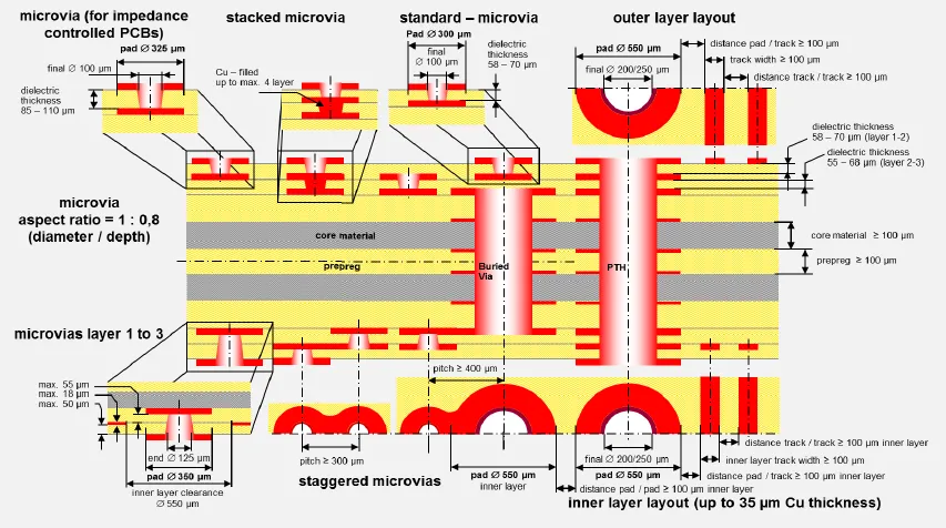
Demystifying Sequential Build Up PCBs: A Beginner's Guide to HDI Technology
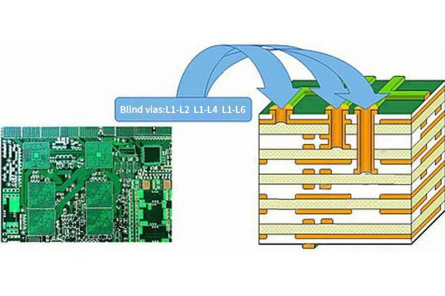
Cost Effective Sequential Build Up PCB Design: Strategies for Reducing Manufacturing Expenses
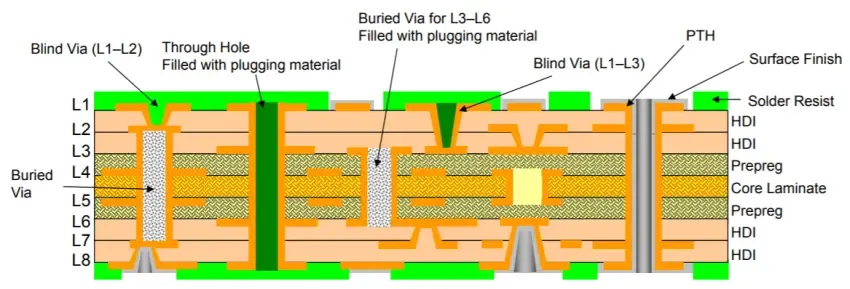
Miniaturized HDI PCB: Design and Manufacturing for Small Form Factor Electronics
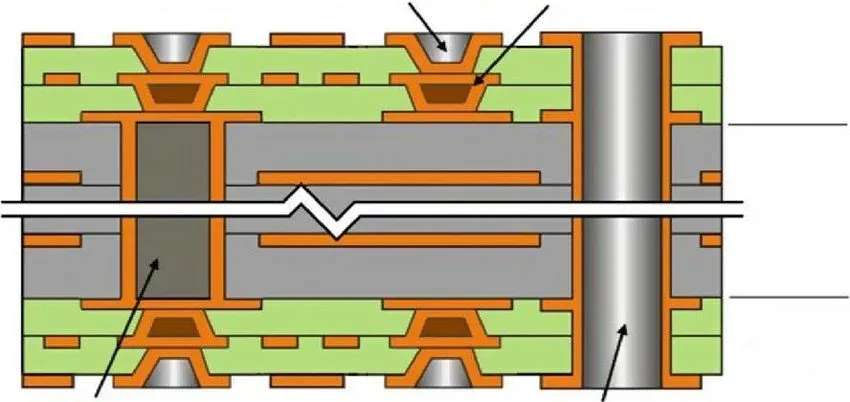
Advanced HDI PCB: Materials, Manufacturing, Design, and Interconnect Technology
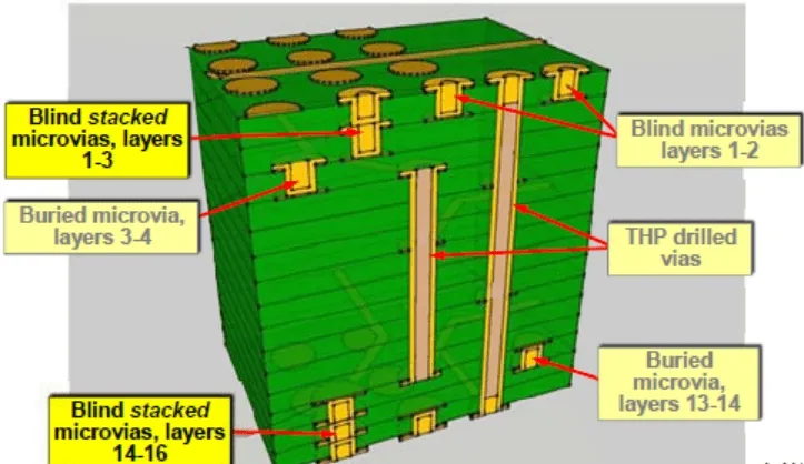
Troubleshooting Stacked Via Problems: A Practical Guide
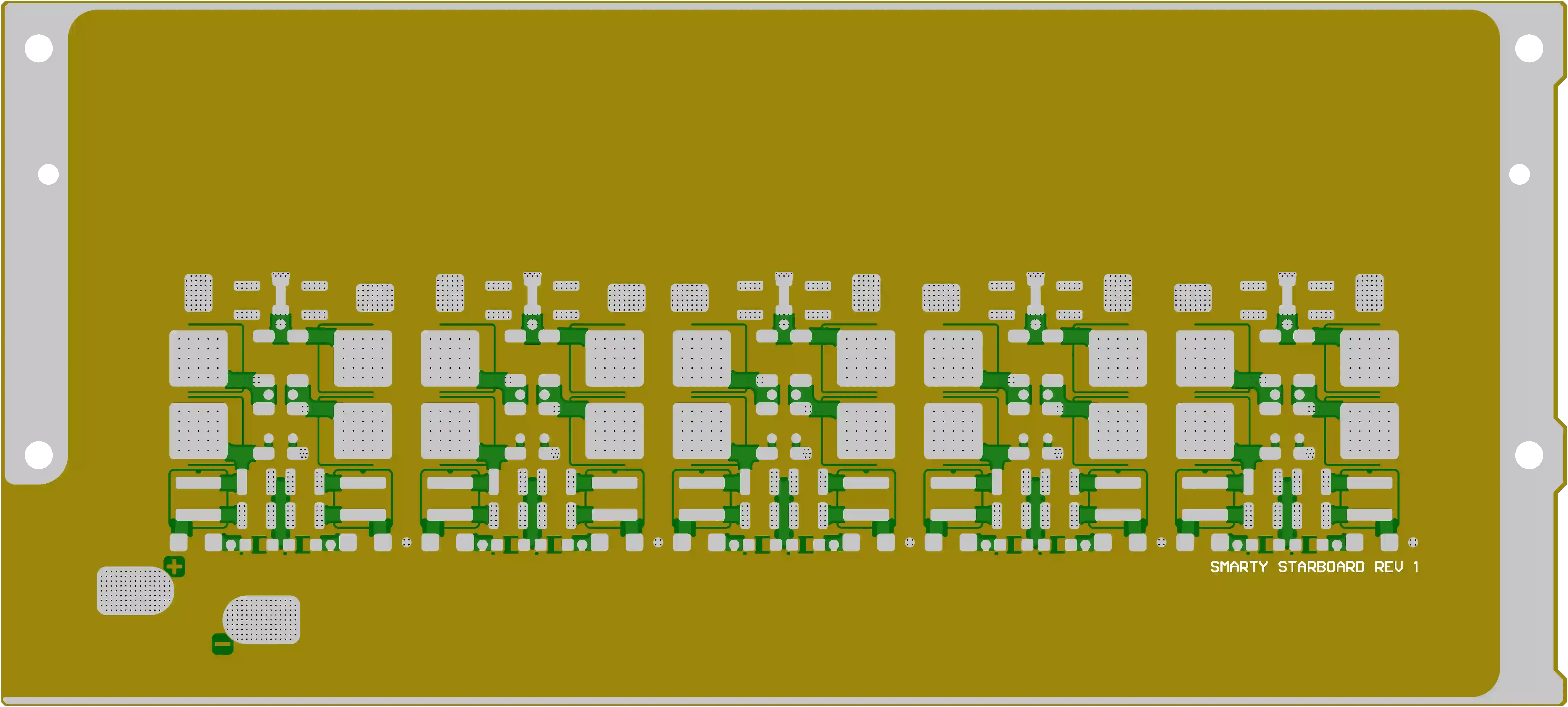
0.15mm Hole & Countersink Depth Control in 4-Layer HDI PCB
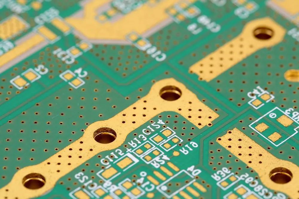
HDI PCB Design With Copper Thickness Options: CAM Review and Manufacturing Control
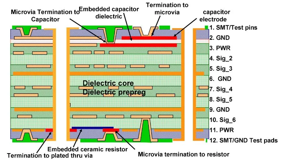
How PCB Manufacturers Improve Solder Mask Yield in HDI Production
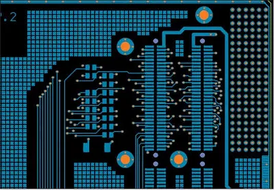
Why HDI PCB Manufacturers Add Dummy Copper
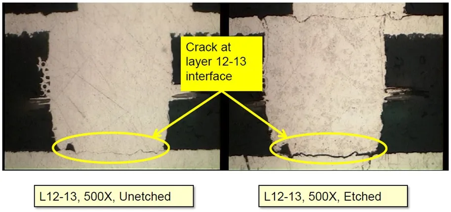
Why HDI Microvias Fail During Production: Common HDI Defects and Causes