02:50
02:50
Via-In-Pad
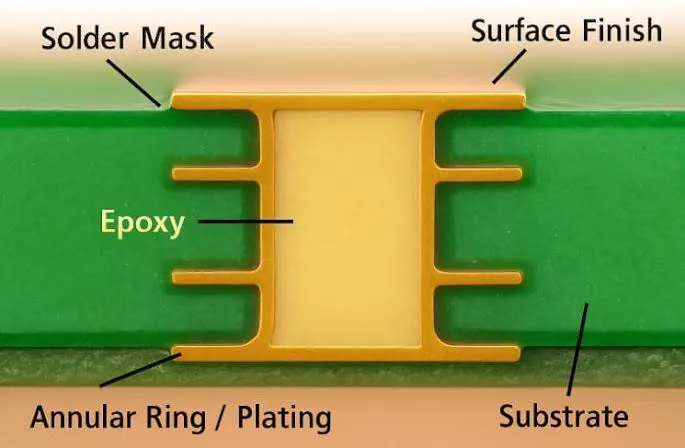
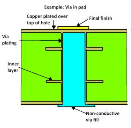
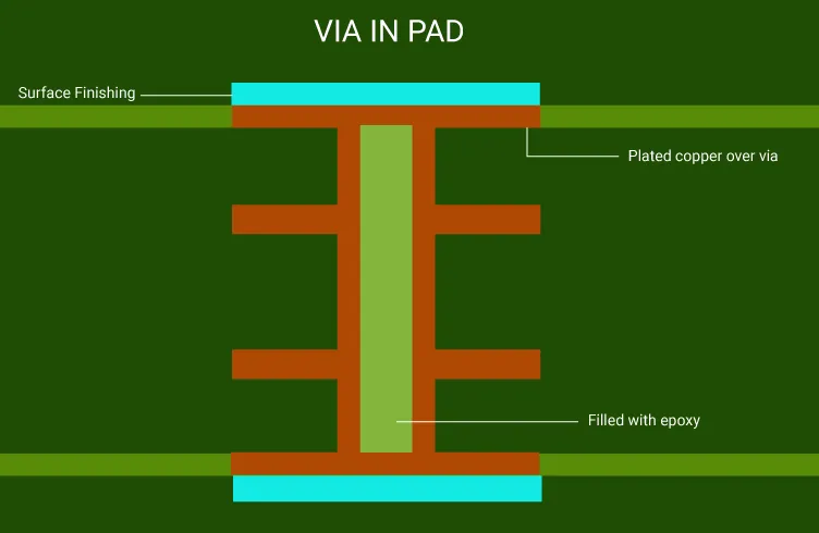
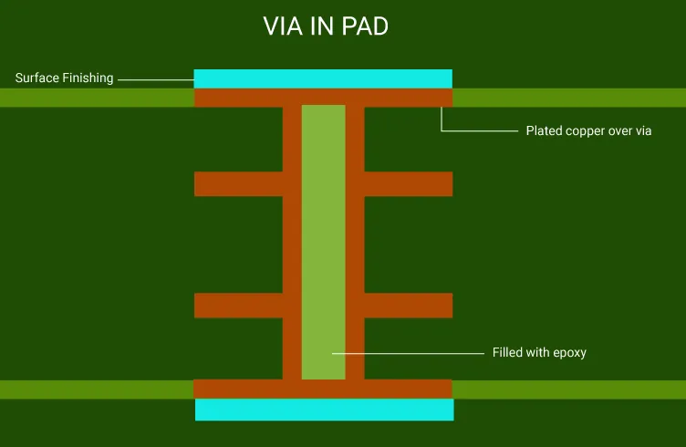
Via-in-pad technology represents a critical advancement in printed circuit board (PCB) design, particularly for high-density applications where space optimization is essential. This technique involves placing vias directly within the component pads, allowing for more efficient routing and reduced board size without compromising electrical performance. Engineers and designers often search for via-in-pad solutions when working on complex layouts, such as those involving ball grid array (BGA) packages, fine-pitch components, or multilayer boards. By integrating vias into pads, it becomes possible to minimize signal path lengths, enhance thermal management, and improve overall board reliability, making it a go-to method for modern electronics like smartphones, automotive systems, and high-speed computing devices. Understanding the practical applications of via-in-pad can significantly impact your PCB projects. For instance, in designs requiring high signal integrity, this approach helps reduce inductance and crosstalk, leading to better performance in RF and high-frequency circuits. It also facilitates easier assembly processes, as filled or plugged vias prevent solder wicking and ensure flat surfaces for component placement. However, successful implementation demands careful consideration of manufacturing constraints, such as via filling materials and plating techniques, to avoid issues like voids or reliability failures over time. To achieve optimal results, adhere to best practices like selecting appropriate via sizes based on current requirements and ensuring compatibility with your fabrication partner's capabilities. Testing for thermal cycling and mechanical stress is advisable to validate long-term durability. For those delving deeper into PCB design strategies, the articles linked under this tag offer detailed case studies, tutorials, and expert tips that can guide you through real-world implementations and troubleshooting. Whether you are refining an existing design or starting a new one, these resources provide the insights needed to leverage via-in-pad effectively.
Video Guide
-
02:50
-
 00:54
00:54
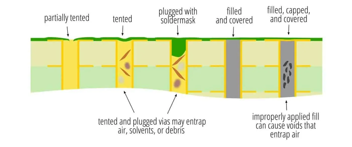
Via Tenting vs Resin Plugging: When Do You Need Resin Filling for Via-in-Pad Designs?
-
 00:45
00:45
The Fastest Way to Waste Money on Your First PCB
-
 00:54
00:54
PCB Vias: Critical Design Factors for Manufacturing Yield and Reliability
-
 00:59
00:59
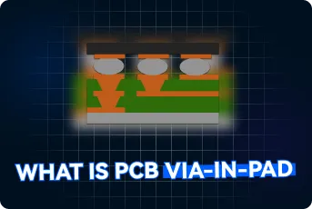
Via-in-Pad for BGA PCBs: When to Use It and Critical DFM Rules
Technical Articles
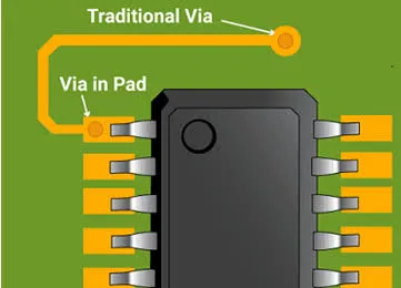
Via-in-Pad vs Traditional Via Routing for HDI PCB
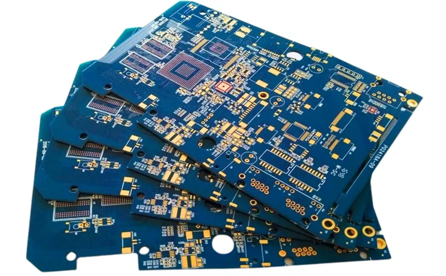
Common Via-in-Pad Design Mistakes in HDI PCB
Resin Filled Via vs Copper Filled Via HDI: What Is the Difference?
Overcoming Solder Wicking in Via in Pad: Techniques and Solutions
Creating Your First Via in Pad PCB: A Step by Step Guide
Enhancing PCB Reliability with Via in Pad Technology
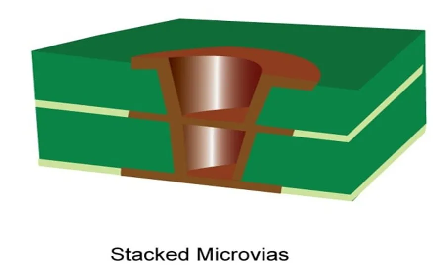
Stacked Via vs. Via in Pad: Which Via Technology is Best for BGA Routing?
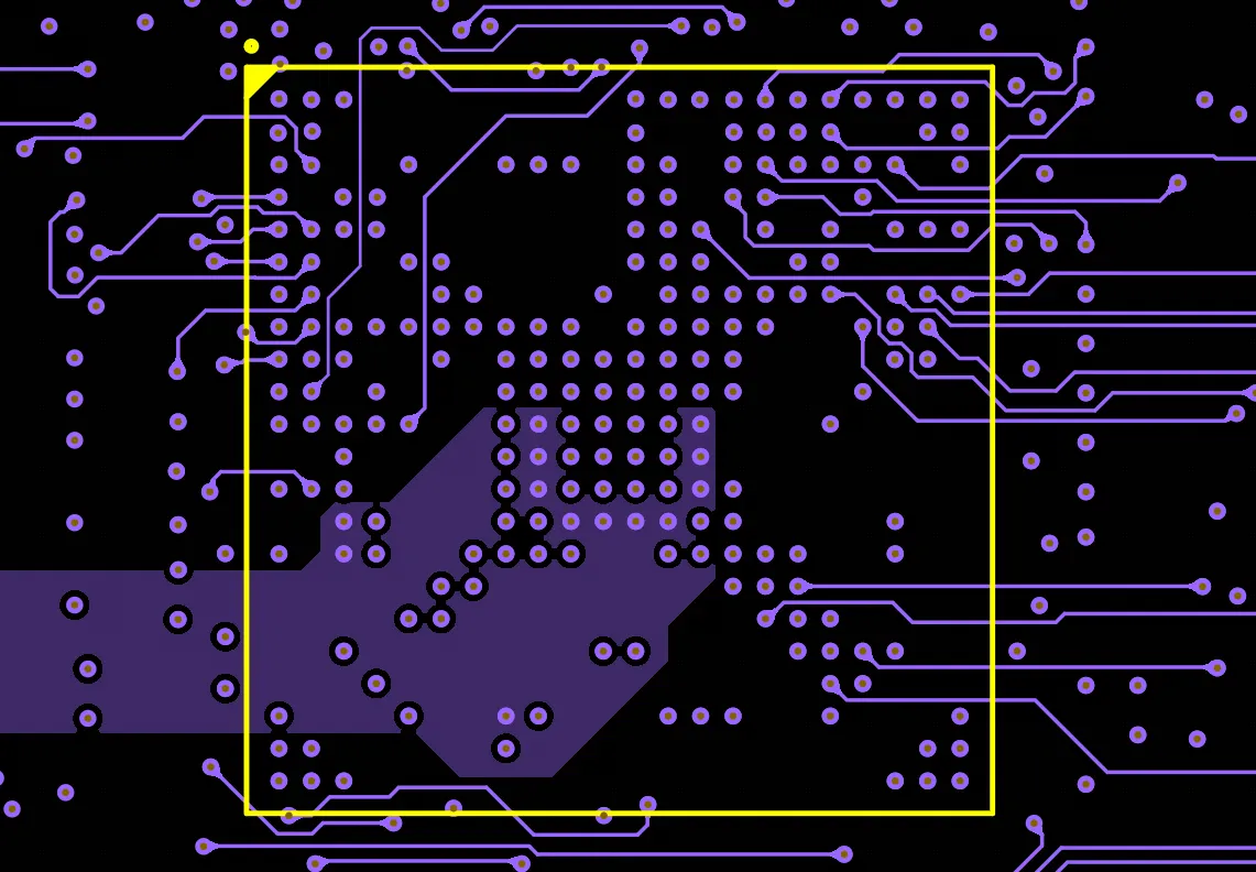
Basics of routing with BGA packages
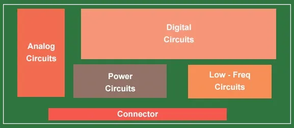
HDI Multilayer PCB Design: Advanced Techniques for High-Density Boards
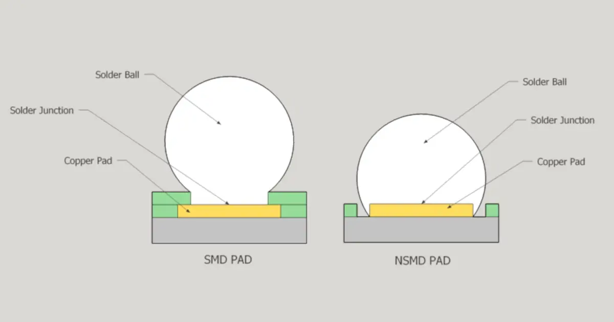
Fanout and routing: How to connect BGA packages to the rest of the PCB
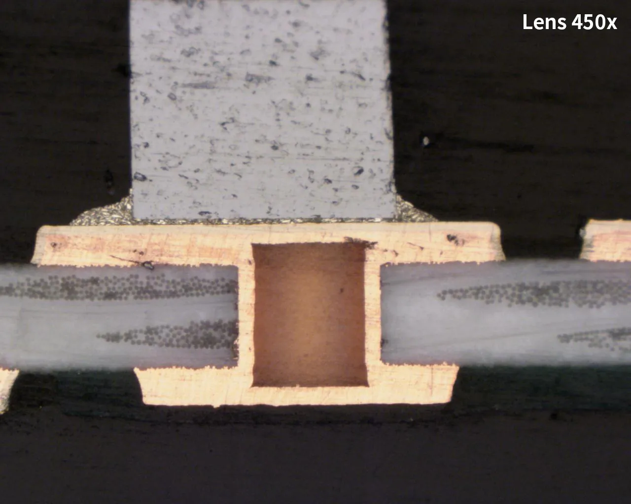
The Role of Via Filling in Via in Pad Reliability
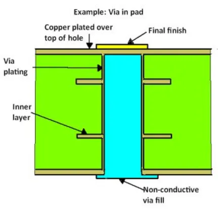
Via in Pad Alternatives: When to Choose a Different Via Structure
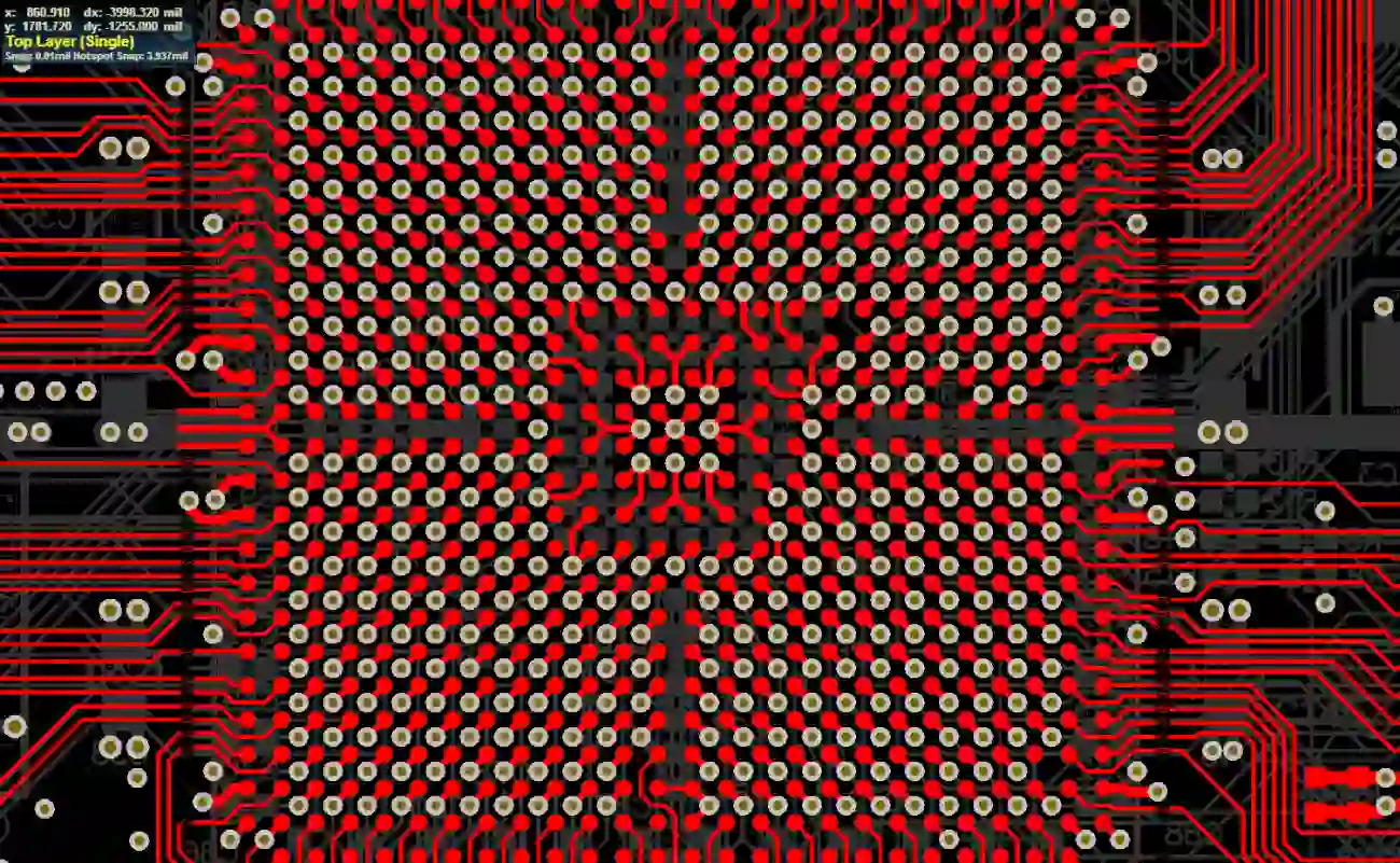
Signal Integrity Showdown: Via in Pad vs. Dog Bone Routing
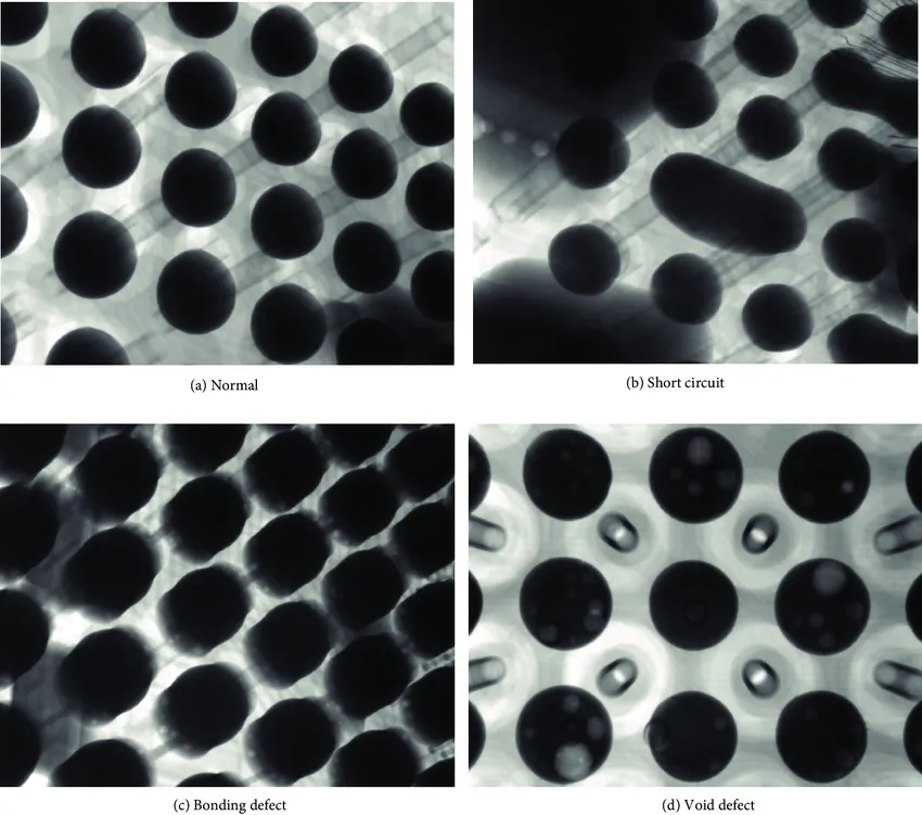
HDI PCB X-Ray Inspection for Assemblies: SMT Defect Detection and Quality Control
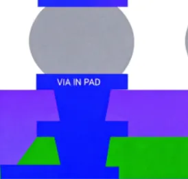
Via in Pad: Maximizing Density and Performance in Advanced PCB Designs
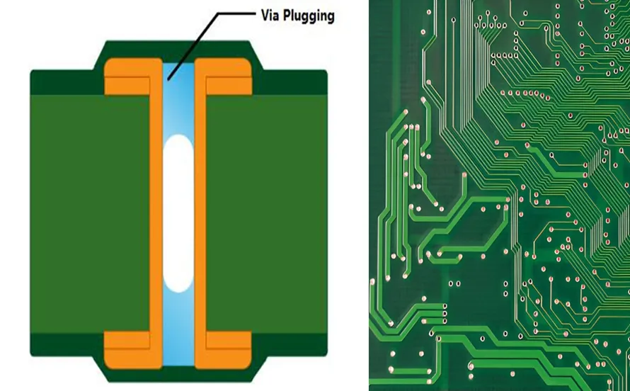
Boosting PCB Reliability: How Via Filling Prevents Solder Wicking and Contamination
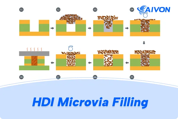
The Ultimate Guide to PCB Microvia Filling: Materials, Methods, and Reliability Considerations
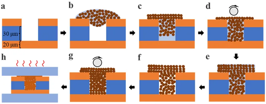
Sequential Lamination and Via in Pad: Maximizing Component Density on HDI PCBs
Via-in-Pad Without Fanout Advantages and Disadvantages