 12:36
12:36
Design For Manufacturing
Design for Manufacturing (DFM) is a critical approach in electronics and PCB development that bridges the gap between innovative design and efficient production. By integrating manufacturing considerations early in the design process, engineers can minimize costly revisions, reduce material waste, and ensure smoother assembly lines. This tag page compiles expert insights into DFM principles tailored for PCB designers, hobbyists, and industry professionals seeking to optimize their projects for real-world fabrication. At its core, Design For Manufacturing emphasizes practical strategies such as selecting appropriate component footprints, optimizing panelization for high-volume runs, and adhering to fabrication tolerances that prevent defects like soldering issues or mechanical failures. For instance, incorporating generous clearances around vias and traces can significantly enhance yield rates during automated assembly, while choosing standard materials helps control costs without sacrificing performance. These best practices not only accelerate time-to-market but also improve product reliability, making them essential for anyone involved in prototyping or scaling electronics production. Whether you are troubleshooting a design that failed in manufacturing or looking to refine your workflow for better efficiency, the articles linked here offer step-by-step guidance on implementing DFM in tools like Altium or KiCad. Delve into case studies that demonstrate how small adjustments in layout can lead to substantial savings, or learn about common pitfalls to avoid in multilayer board designs. This collection serves as a valuable resource for enhancing your expertise and achieving manufacturable designs that meet both technical and economic goals.
Video Guide

Technical Articles
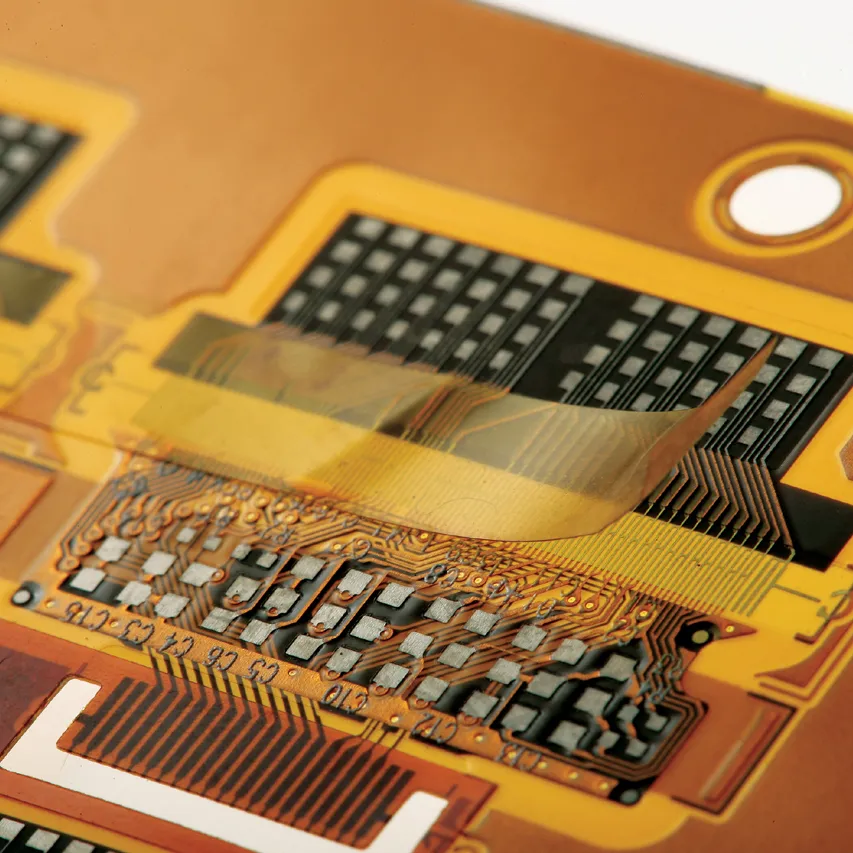
FPC Tape: Why Flush Edges Cause Adhesive Overflow
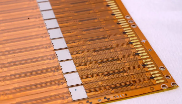
FR4 Stiffener Inner Shrink Rule for FPC Boards
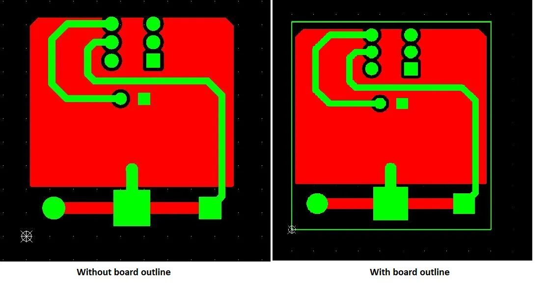
Common Outline Layer Mismatch Problems in FPC Gerber Files
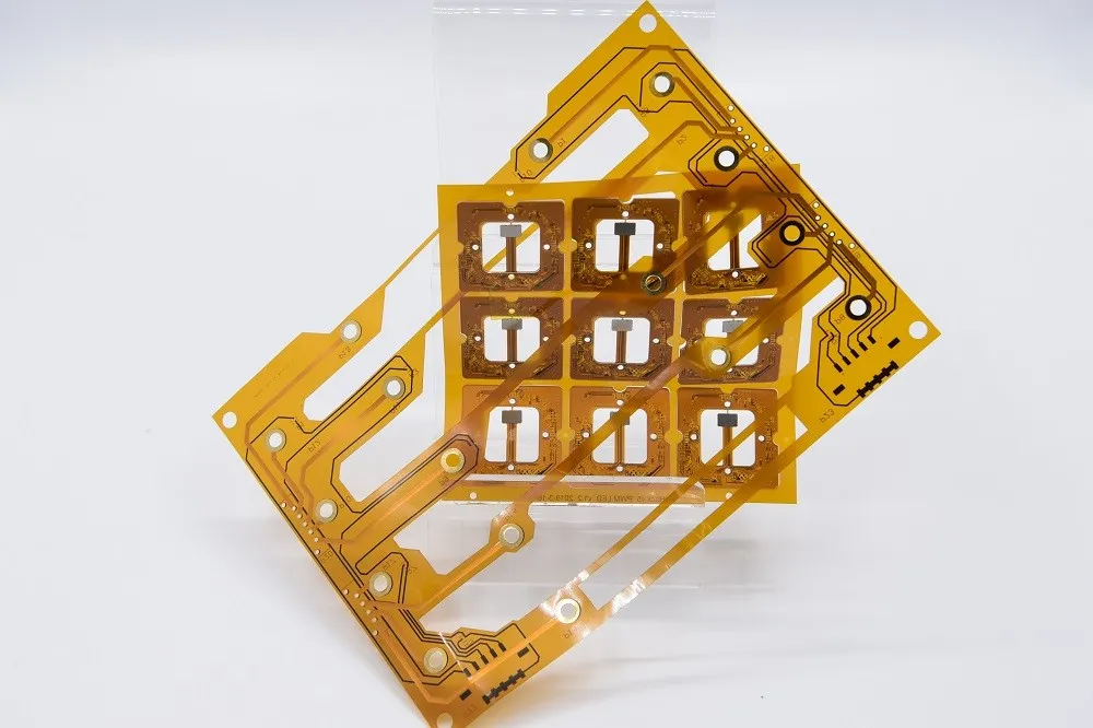
Why Large Ground Openings Can Cause Manufacturing Problems in FPC?

How Many Connection Points Are Needed for Stable FPC Panel Shipment?
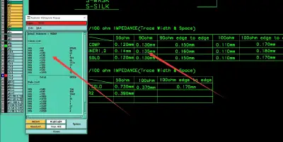
Why Impedance Line Mismatches Triggered EQ in Multi-Layer PCB Production
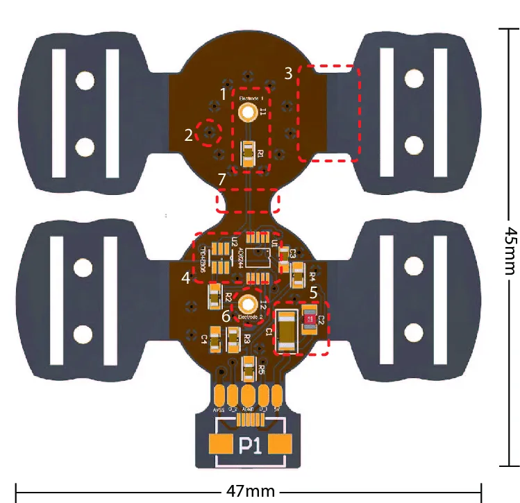
What Happens When FPC Characters Are Placed on or Too Close to Pads
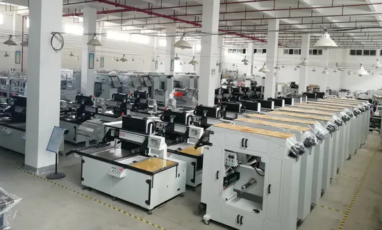
Why FPC Silkscreen Characters Keep Coming Out Blurry
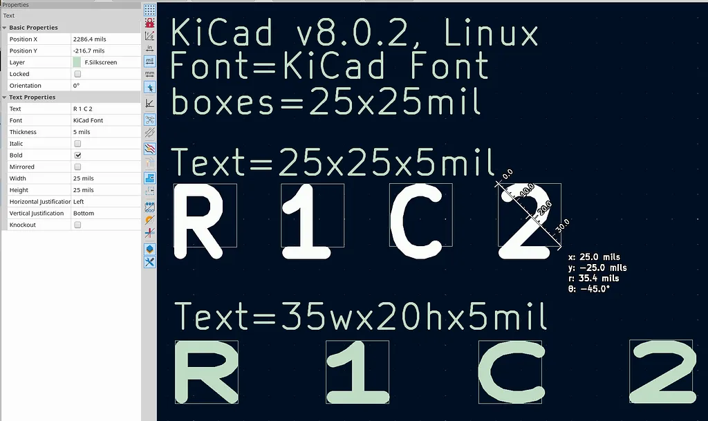
How Small Is Too Small for FPC Legend Text?
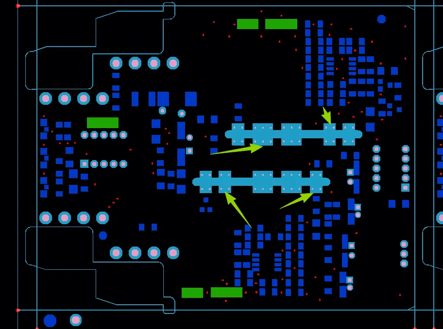
How DFM Review Prevented Via Reliability Risks in a 2-Layer FR4 PCB
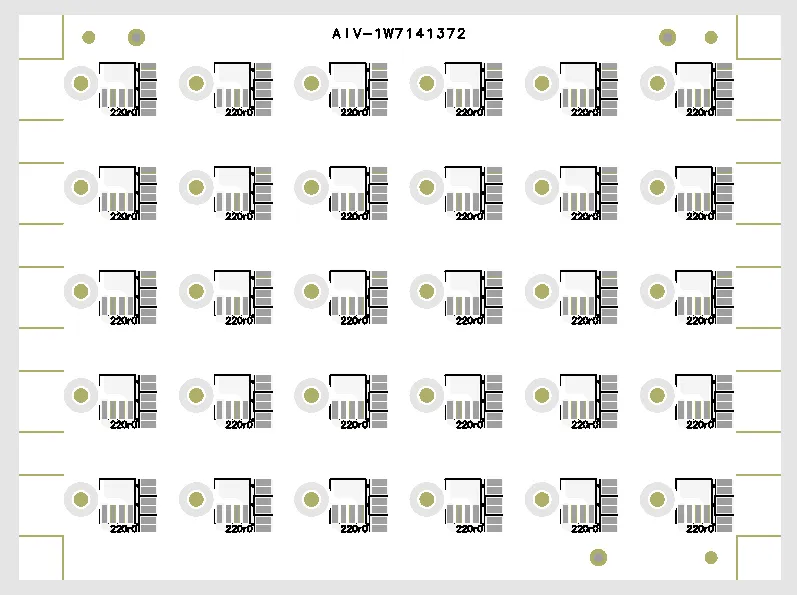
Preventing Edge Breakout and Burr Risks in Aluminum PCB Panelization
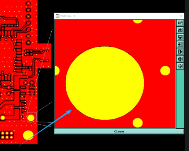
Preventing Exposed Copper and Via Plugging Risks in a Compact 4-Layer FR4 PCB

Troubleshooting Firewall Login Failures

Building a Portable Load Scale with HX711, Arduino, and Load Cells: PCB Design Insights

Open-source Industrial PLM: Accessing DocDoku-PLM Source

FR4 PCB Minimum Trace Width: What Designers Should Know

FR4 PCB Annular Ring: Design Rules and Reliability Considerations

FR4 PCB Via Size and Pad Size: How to Choose the Right Dimensions
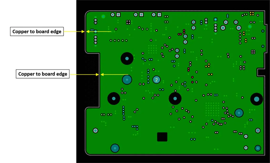
FR4 PCB Edge Clearance: How Much Copper Should Be Kept from the Board Edge?