 12:36
12:36
Design For Manufacturing
Design for Manufacturing (DFM) is a critical approach in electronics and PCB development that bridges the gap between innovative design and efficient production. By integrating manufacturing considerations early in the design process, engineers can minimize costly revisions, reduce material waste, and ensure smoother assembly lines. This tag page compiles expert insights into DFM principles tailored for PCB designers, hobbyists, and industry professionals seeking to optimize their projects for real-world fabrication. At its core, Design For Manufacturing emphasizes practical strategies such as selecting appropriate component footprints, optimizing panelization for high-volume runs, and adhering to fabrication tolerances that prevent defects like soldering issues or mechanical failures. For instance, incorporating generous clearances around vias and traces can significantly enhance yield rates during automated assembly, while choosing standard materials helps control costs without sacrificing performance. These best practices not only accelerate time-to-market but also improve product reliability, making them essential for anyone involved in prototyping or scaling electronics production. Whether you are troubleshooting a design that failed in manufacturing or looking to refine your workflow for better efficiency, the articles linked here offer step-by-step guidance on implementing DFM in tools like Altium or KiCad. Delve into case studies that demonstrate how small adjustments in layout can lead to substantial savings, or learn about common pitfalls to avoid in multilayer board designs. This collection serves as a valuable resource for enhancing your expertise and achieving manufacturable designs that meet both technical and economic goals.
Video Guide

Technical Articles
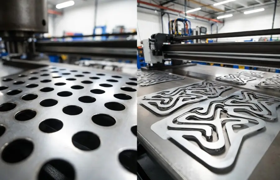
Laser Cutting vs CNC Punching for Sheet Metal Parts: Which One Should You Choose?
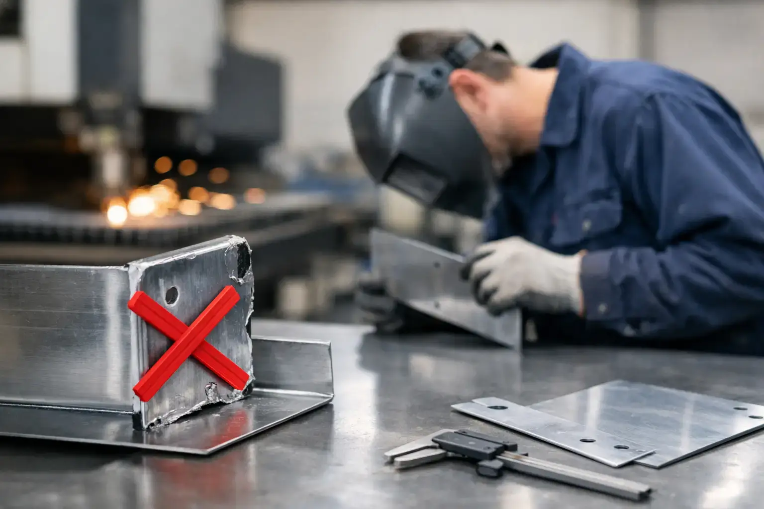
7 Common Surface Finish Mistakes in Sheet Metal Fabrication
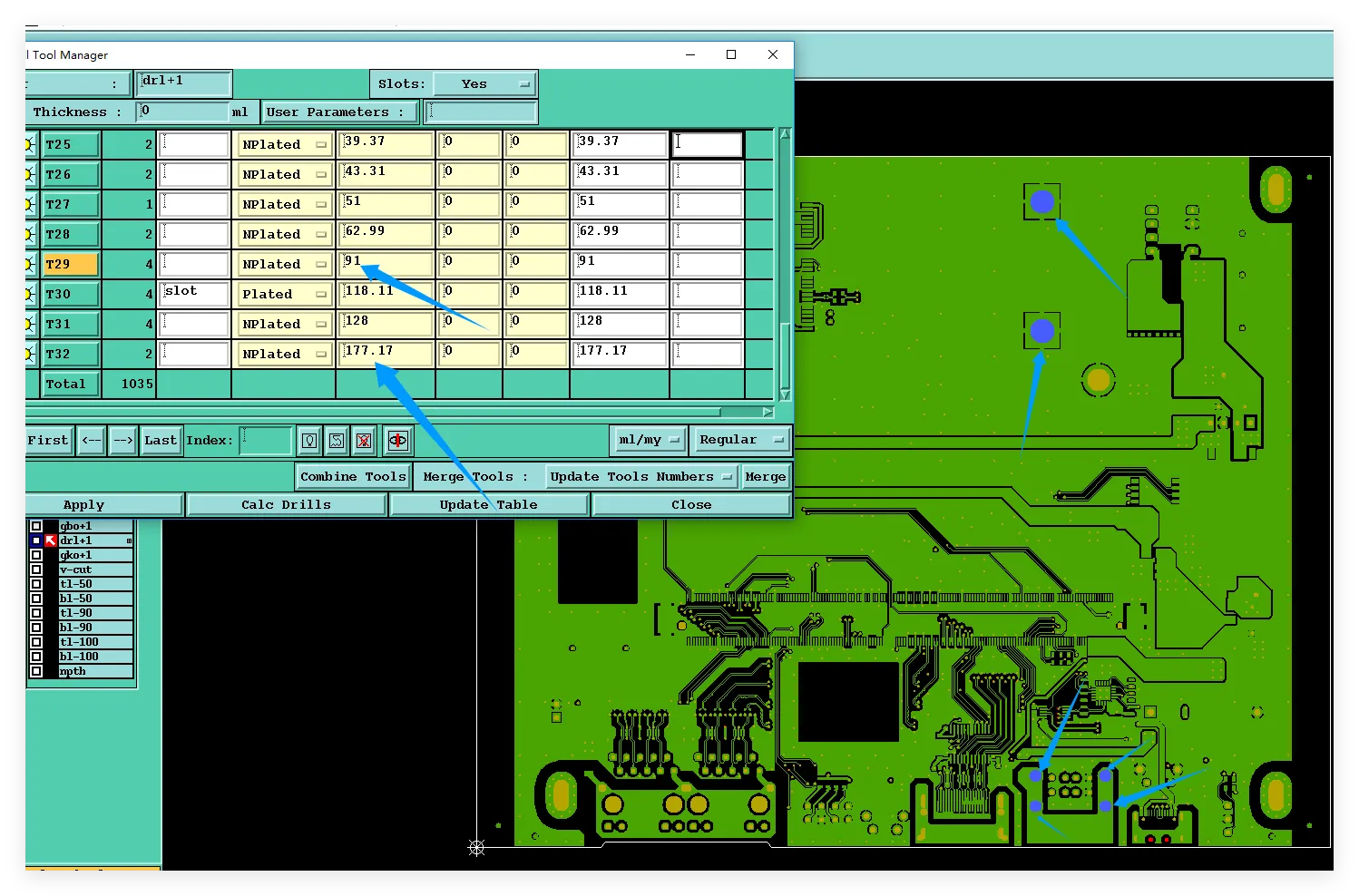
PCB Via-in-Pad Design Rules: Avoiding SMT Assembly Voids
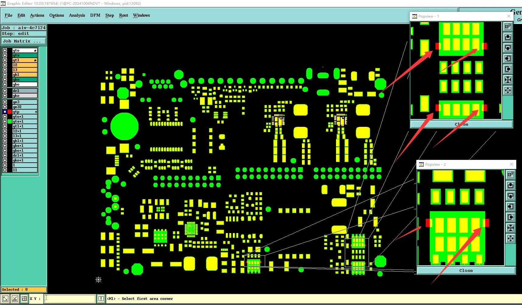
Solder Mask vs. Paste Mask: Perfecting Your Opening Design
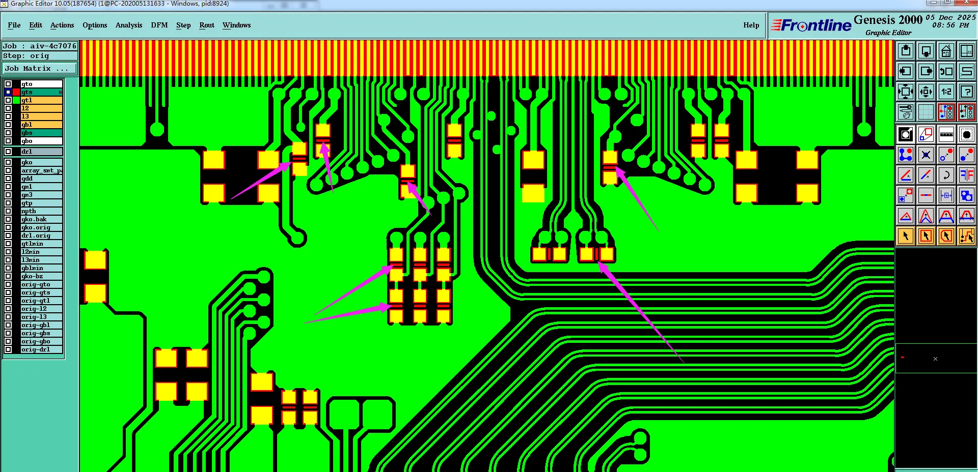
How DFM Prevented SMT Shorts from Narrow Mask Bridges
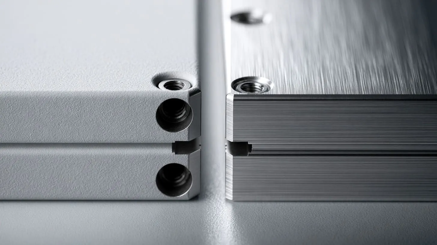
Powder Coating vs Anodizing for Sheet Metal Parts: Which Finish Is Better?
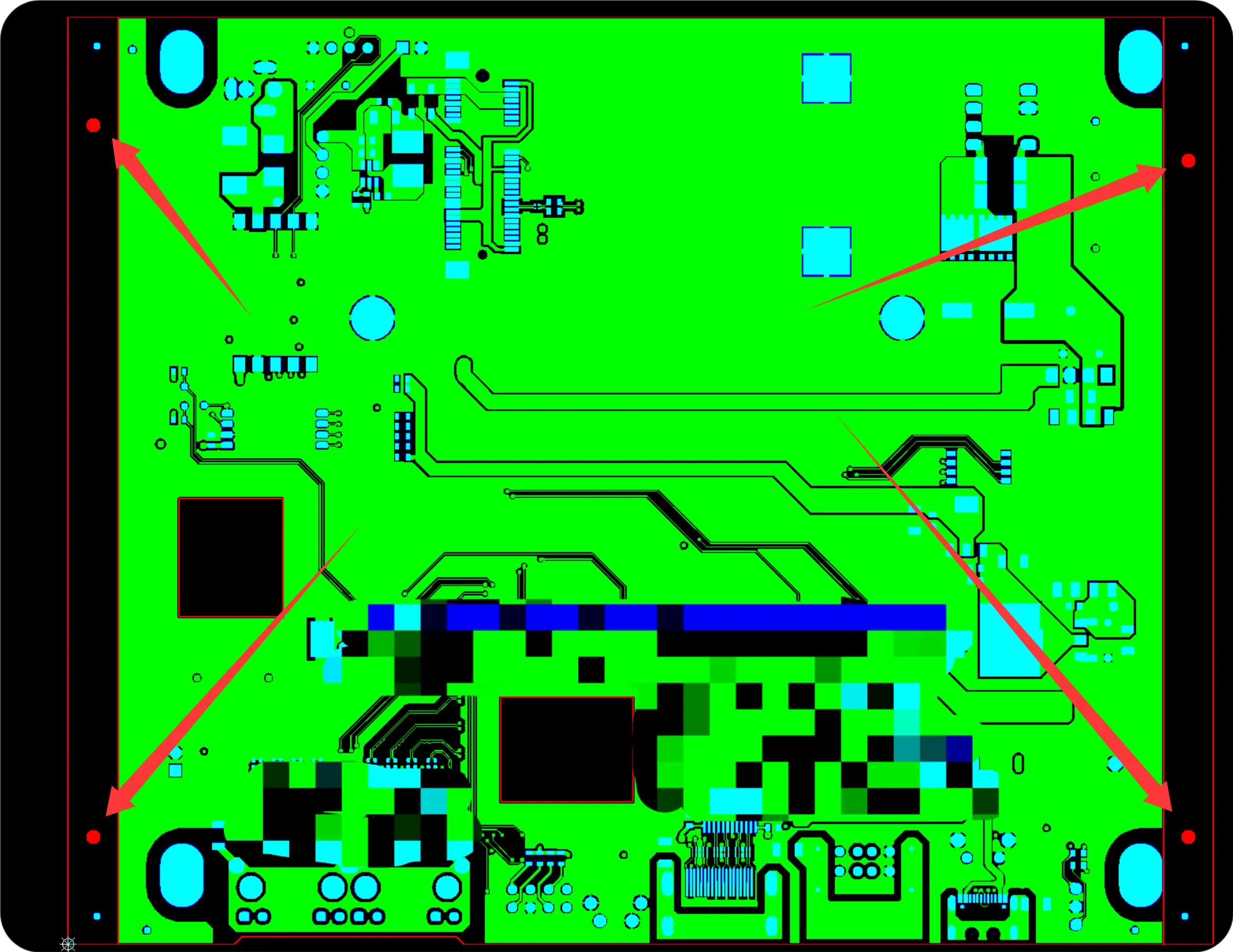
Handling PCB Impedance Trace Width Adjustment in DFM Review
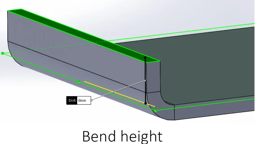
Sheet Metal Flange Design Guidelines: Height, Length and Bend Considerations
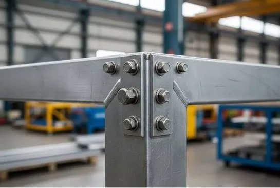
Sheet Metal Assembly Design Guide: Fasteners, Inserts and Joining Methods

10 Common Electronic Enclosure Design Mistakes That Increase Manufacturing Costs

How to Choose the Right Surface Finish for CNC Parts
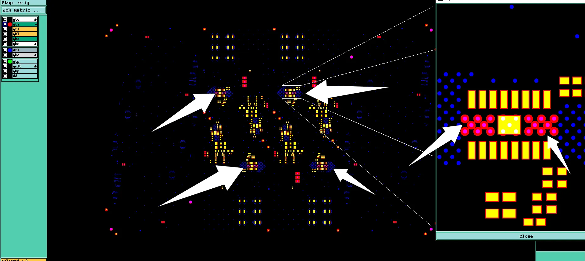
Resolving Tented Via vs Open Via Mismatches in PCB Manufacturing

CNC Milling vs CNC Turning: What's the Difference?
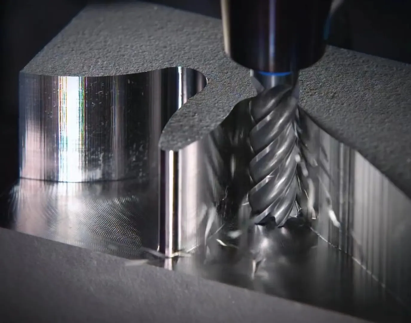
Internal Corner Radius Design Guidelines for CNC Parts
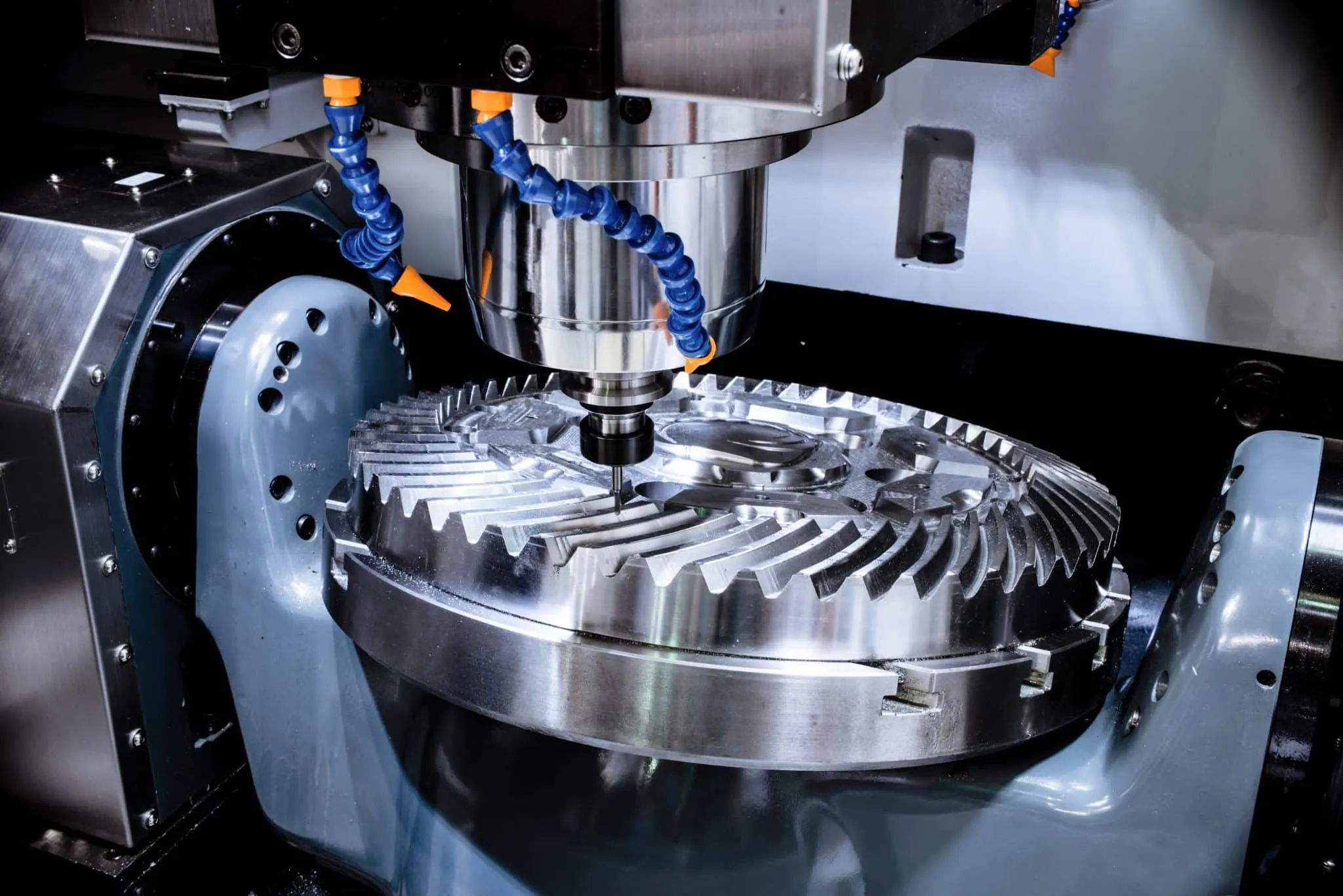
CNC Machining Services Explained: Processes, Capabilities and Applications
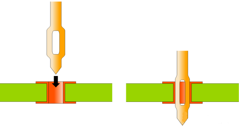
Tight Press Fit Hole Tolerance Triggers EQ in 2-Layer FR-4 PCB
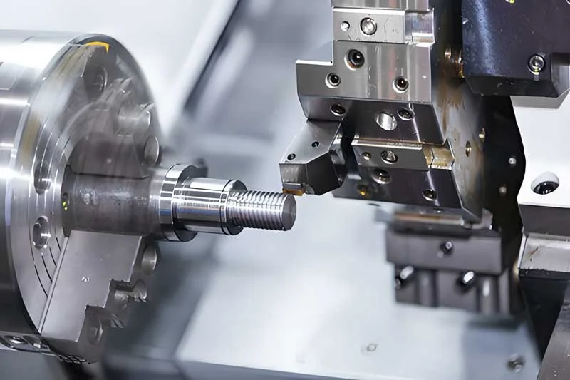
Why Deep Pockets Increase CNC Machining Costs
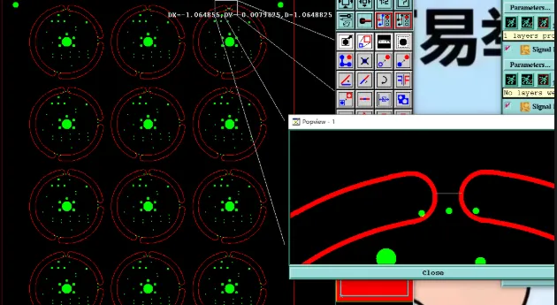
Undersized Panel Connection Tabs Risk Board Breakage in 2-Layer PCB

How to Design CNC Parts for Low Volume Production