










Differential Pair Routing
Differential pair routing is a critical technique in printed circuit board (PCB) design, where two complementary signal traces are routed together to transmit data with high integrity. This method involves pairing traces that carry equal but opposite signals, allowing common-mode noise to cancel out while preserving the differential signal. Engineers and designers searching for information on differential pair routing often seek ways to enhance signal quality in high-speed applications, such as USB, HDMI, Ethernet, and DDR memory interfaces. By implementing this approach, you can significantly reduce electromagnetic interference (EMI), crosstalk, and signal distortion, which are common challenges in dense, fast-paced electronic systems. In practice, effective differential pair routing requires attention to several best practices to achieve optimal performance. Key considerations include maintaining equal trace lengths to avoid skew, ensuring consistent spacing between the pairs for impedance control, and minimizing vias or layer transitions that could introduce discontinuities. For instance, in multilayer PCBs, routing differential pairs on adjacent layers with ground planes can help shield against external noise. Tools like simulation software can aid in verifying impedance matching and predicting signal behavior before fabrication, saving time and costs during prototyping. These techniques are especially valuable in industries like telecommunications, automotive electronics, and consumer devices, where reliable data transmission is essential for functionality and compliance with standards such as those from the IPC. This tag page gathers a collection of articles that delve into the nuances of differential pair routing, offering step-by-step guidance, case studies, and troubleshooting tips. Whether you are optimizing a new design or refining an existing one, these resources provide the insights needed to implement robust routing strategies and improve overall PCB performance.
Technical Articles

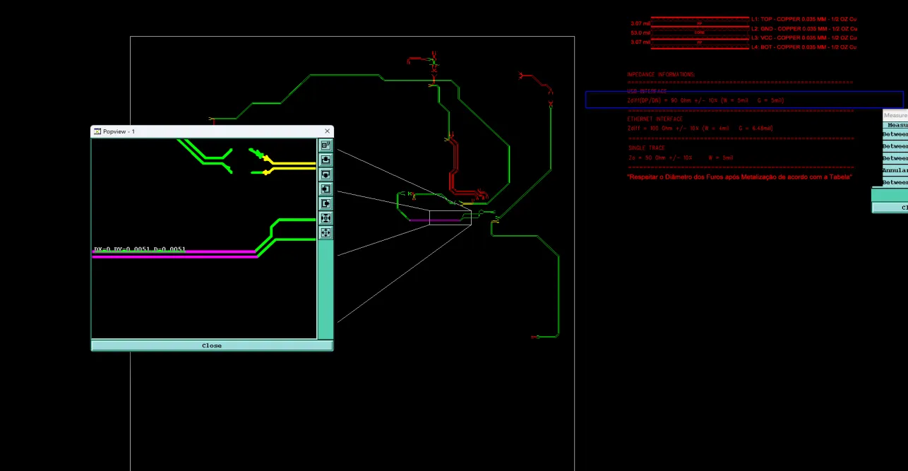
PCB Layout and Routing Requirements for USB 2.0, USB 3.0, and USB Type C Interfaces

Cadence Allegro PCB Multi?Trace Routing and Spacing Control
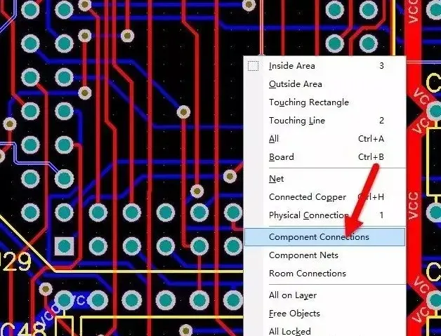
Selecting and Unrouting Nets Associated with a Component in PCB Layout
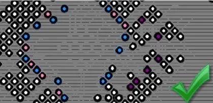
DDR Module PCB Design: Topologies, Routing Rules, and Skew Control
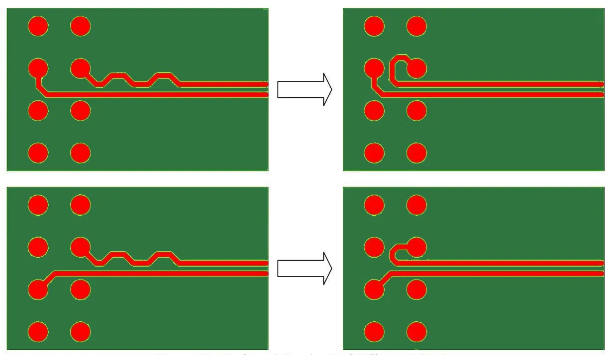
11 Best Practices for High-Speed PCB Routing (Part 1)
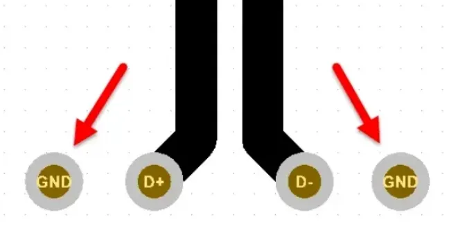
USB Interface PCB Design Guide: From Type-C to High-Speed Routing
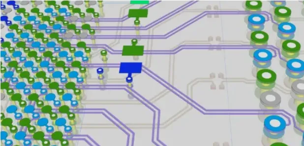
Defining and Using Differential Pairs in KiCad
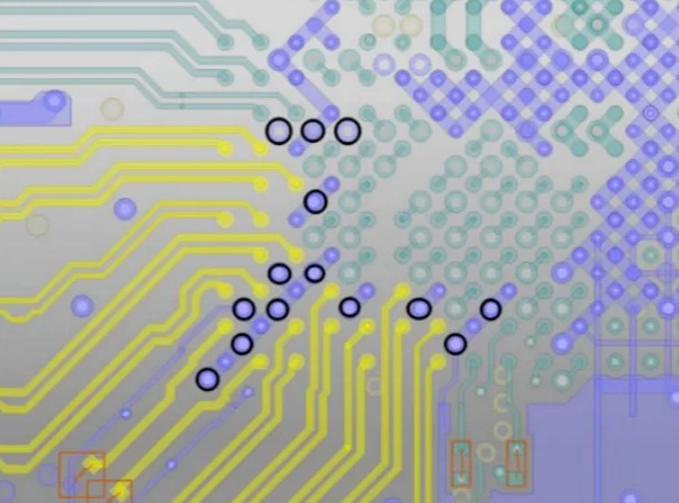
PCB Layout and Routing Requirements for PCIe Interfaces
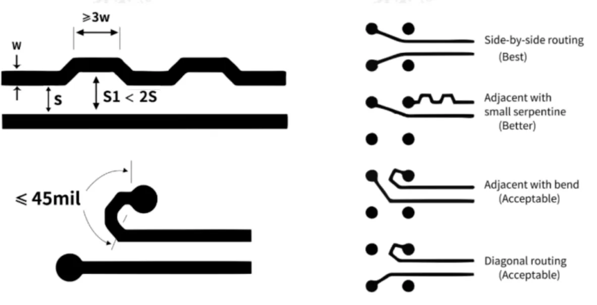
PCB Layout and Routing Requirements for a DP 1.4 Interface
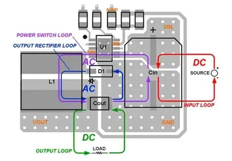
15 PCB Layout Techniques for EMC Control
Basic PCB Concepts Needed to Start a Design

Stop Drawing Arbitrary Serpentine Traces: The Real Constraint in PCB Length Matching
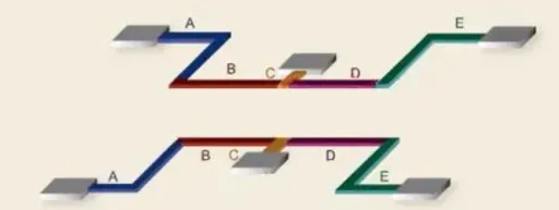
PCB Design Keep Going Wrong? 13 Key Fundamentals That Build a Solid Baseline
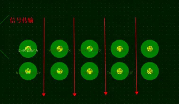
High-Speed PCB Vias: A Small Feature That Can Break the Signal
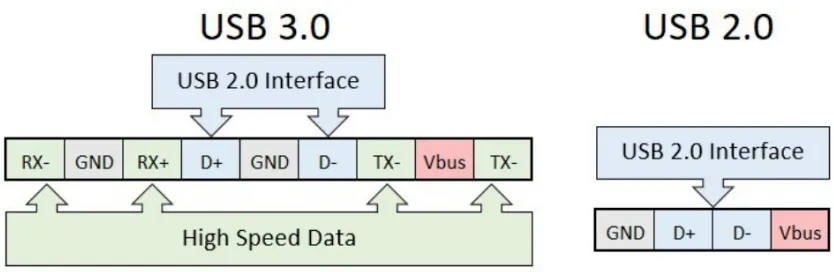
A USB Port Looks Simple. A Bad PCB Layout Turns It Into a Signal Problem
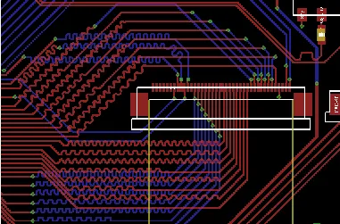
FR4 PCB Differential Pair Routing: Spacing and Length Matching
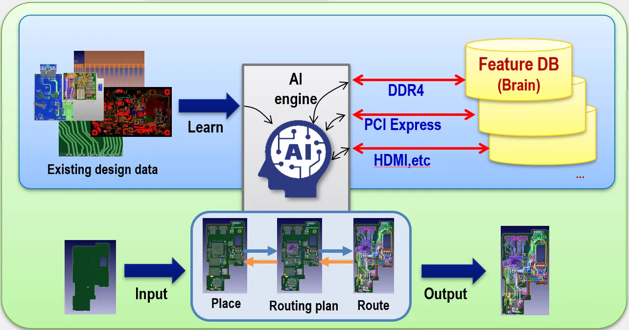
How AI Can Assist Multilayer PCB Routing and Design

PCB Design Guidelines: Key Routing and Layout Considerations


