 01:02
01:02
Ground Planes
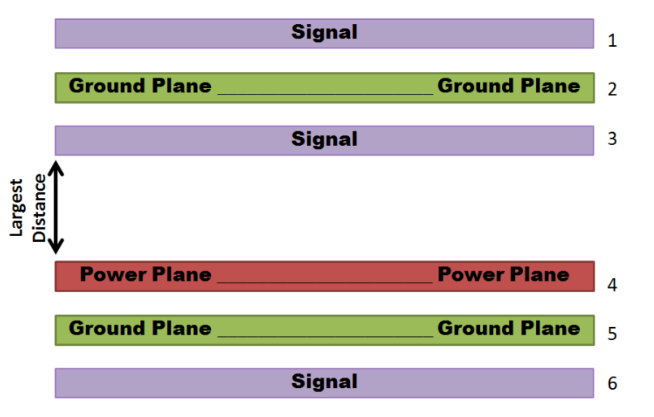
Ground planes are a fundamental element in printed circuit board (PCB) design, serving as expansive layers of conductive material, typically copper, that connect to the circuit's ground reference. They provide a low-impedance return path for electrical currents, which helps minimize noise, reduce electromagnetic interference (EMI), and improve overall signal integrity. For engineers and hobbyists searching for information on ground planes, this tag aggregates articles that delve into their implementation, from basic concepts to advanced techniques in multilayer PCBs. Understanding ground planes is crucial for achieving reliable performance in electronic systems. In high-speed digital circuits, for instance, a well-designed ground plane can prevent issues like ground bounce and crosstalk by ensuring uniform potential across the board. Practical applications include their use in RF designs to shield sensitive components and in power electronics to manage heat dissipation effectively. Best practices often involve maintaining continuous planes without unnecessary splits, strategically placing vias for interconnections, and considering layer stacking to optimize impedance control. These approaches not only enhance circuit stability but also contribute to compliance with industry standards such as those for EMC testing. For those troubleshooting PCB layouts or embarking on new projects, the resources here offer actionable insights, such as guidelines for simulating ground plane effects using tools like SPICE or Altium Designer. By reviewing the articles linked under this tag, you can gain a deeper appreciation of how ground planes influence real-world designs, whether in consumer electronics, automotive systems, or telecommunications equipment. This knowledge empowers you to make informed decisions that elevate the quality and efficiency of your PCB work.
Video Guide
-
01:02
Technical Articles
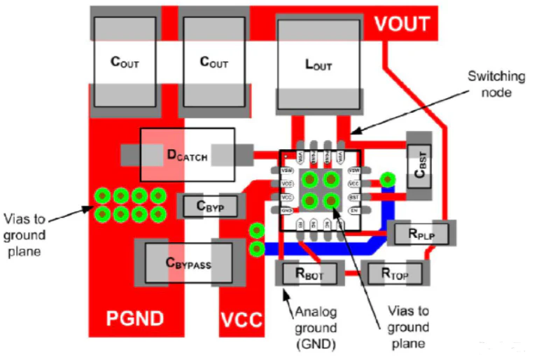
Ground plane for beginners: Making your first circuit!
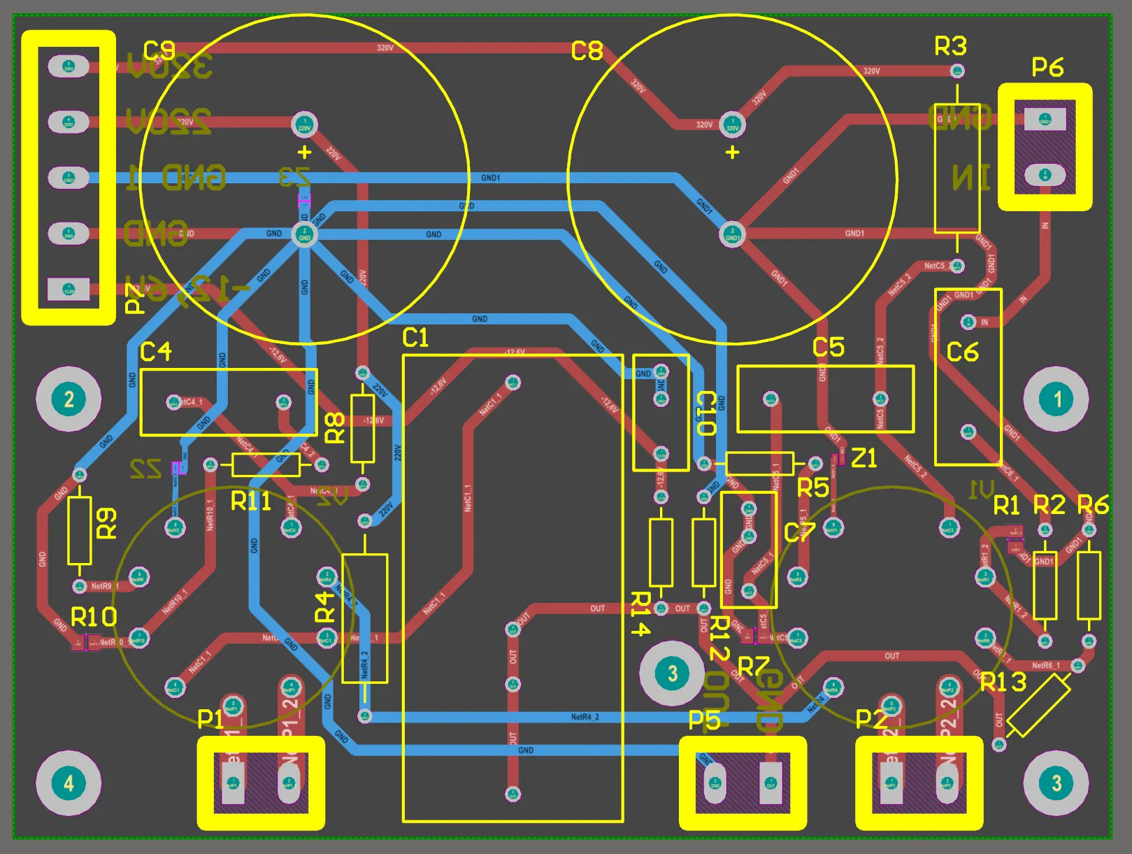
Improve Your Designs with the Best PCB Grounding Techniques
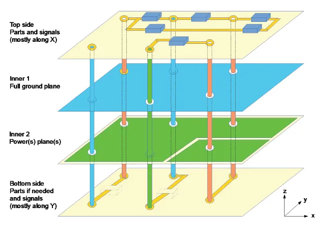
PCB Ground Planes – What are They and Why are They Important?
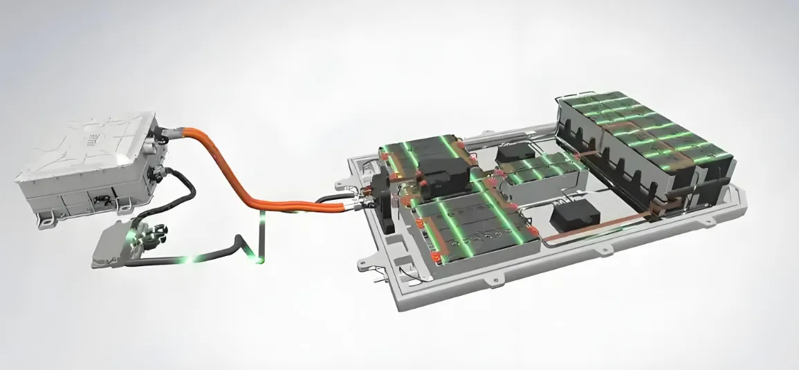
Best Practices for Grounding Strategies in EV Battery Management PCB Designs
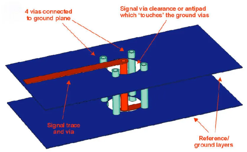
Understanding Power and Ground Planes in Multi Layer PCBs
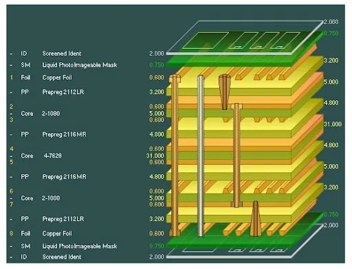
Ground and Power Structures and Routing on Multi Layer Boards
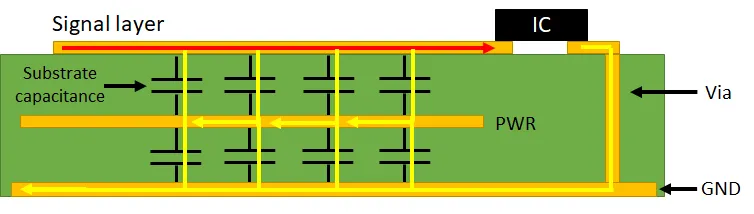
Optimizing Power and Ground Planes in Stackup for Better Circuit Performance
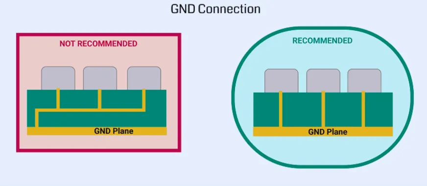
PCB Grounding Techniques: A Guide to Minimizing Noise and Ensuring Reliable Connections
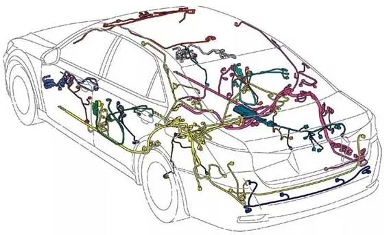
Grounding Design for Automotive Wiring Harnesses
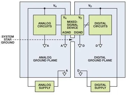
Power and Ground Plane Design in 4 Layer PCBs
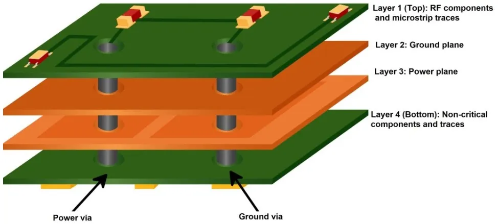
Demystifying Inner Layer Copper Pouring for Hobbyist PCBs
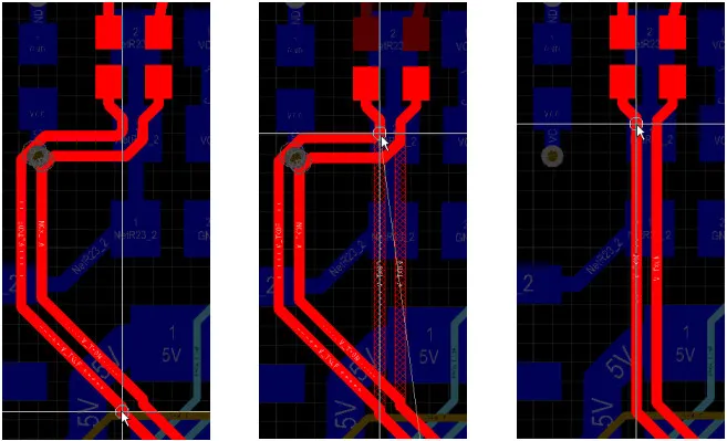
Maximizing Efficiency: Effective Strategies for PCB Routing
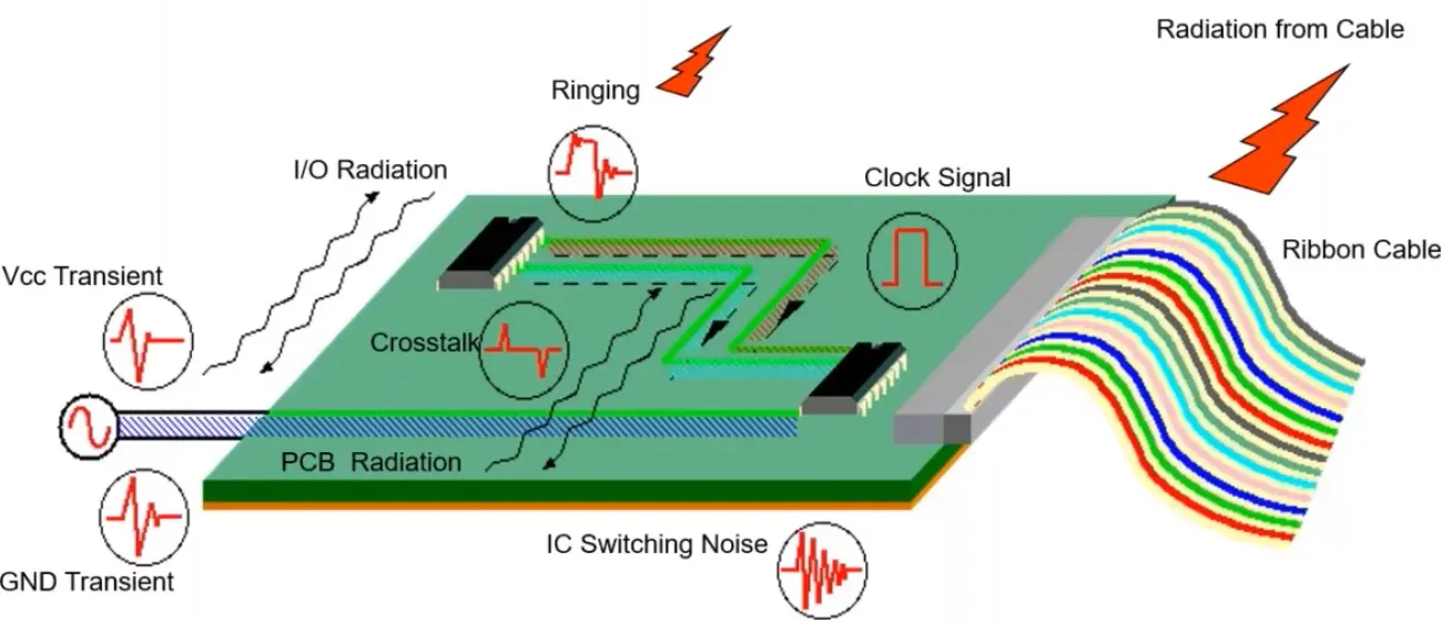
EMI and EMC Compliance 101 for PCB Designers
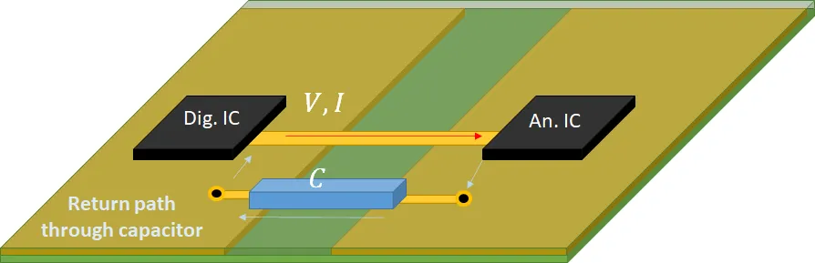
The Art of Grounding: PCB Ground Plane Techniques for Analog Circuits
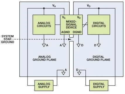
PCB Ground Plane Stack Up: Choosing the Right Configuration for Your Design
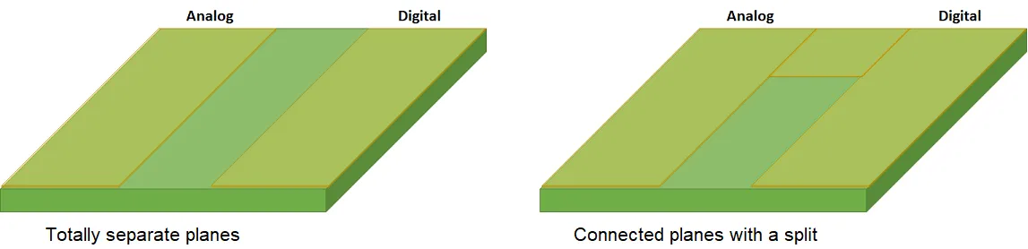
PCB Ground Plane Splits: When to Use Them and How to Avoid Disasters

Measuring Ground Resistance with a Ground Tester
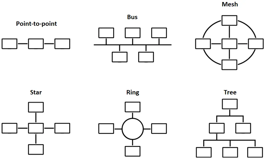
The Art of PCB Trace Routing: Topologies, Techniques, and Best Practices
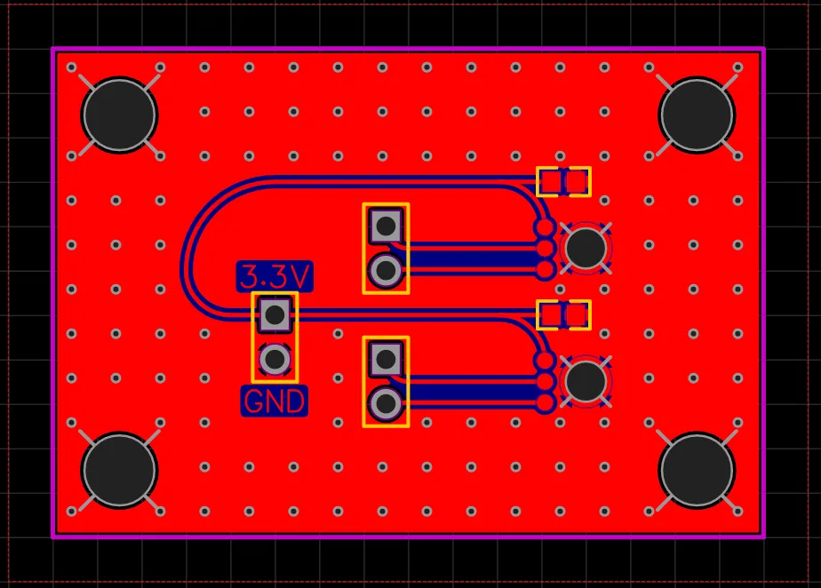
Mastering PCB Copper Pour: Techniques for Effective Grounding and Noise Reduction