


PCB Design
Printed Circuit Board (PCB) design forms the backbone of modern electronics, enabling the creation of compact, efficient, and reliable devices that power everything from smartphones to industrial machinery. In this category, readers gain access to a comprehensive collection of resources dedicated to mastering PCB design principles and techniques. Whether you are a seasoned engineer refining complex layouts or a newcomer learning the fundamentals, these articles provide the knowledge needed to tackle real-world challenges in electronics development. The scope of PCB design covered here extends from initial schematic capture to final board fabrication and testing. Articles delve into essential topics such as layer stacking, signal integrity, thermal management, and component placement strategies. Guides and tutorials offer step-by-step instructions for using popular software tools like Altium Designer and KiCad, while insights explore emerging trends like flexible PCBs and high-speed designs. Best practices emphasize error reduction, cost optimization, and compliance with industry standards, ensuring designs are not only functional but also manufacturable at scale. Real-world applications highlight the category's practical value, demonstrating how effective PCB design contributes to innovations in automotive systems, medical equipment, renewable energy solutions, and consumer gadgets. By addressing common pitfalls and sharing expert tips, these pieces equip professionals to enhance product performance and reliability. Readers benefit from building a deeper understanding through interconnected articles that cover foundational concepts alongside advanced methodologies, fostering continuous improvement in electronics projects. For those involved in prototyping or production, the technical relevance of this content lies in its focus on efficiency and innovation. Detailed discussions on impedance control, EMI shielding, and design for manufacturability prepare you to meet the demands of today's fast-paced tech landscape. Engaging with multiple articles in this category allows for a progressive learning path, where foundational knowledge supports exploration of specialized topics, ultimately leading to more robust and innovative PCB designs.
Featured Blog
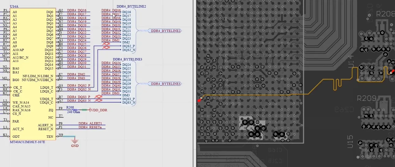
PCB Design Review for Beginners: A Step by Step Guide
Learn how to perform a PCB design review with a practical checklist covering schematics, layout, DRC, manufacturability, and pre-production checks.
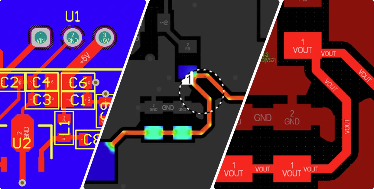
Latest Blogs
Summary | 7 Key Points in PCB Power Design
Seven key PCB power-design considerations: regulator selection, thermal management, power planes, decoupling caps, EMI filtering, frequency response and power integrity.

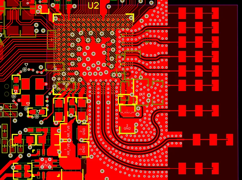
PCB Layout and Routing Requirements for PCIe Interfaces
PCIe PCB layout and routing guidance for PCIe 2.0 and PCIe 3.0, detailing data-rate and encoding differences, BGA fanout, ground-via placement and differential shielding.

Can't Do PCB Layout? This Step-by-Step Guide Makes It Simple
PCB layout guide with practical rules for partitioning, placement, routing, power/ground and thermal design, plus EMC-aware checks to ensure reliable signal performance.
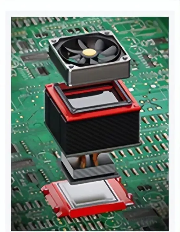
Are PCB Layout and Routing the Same for Industrial-Grade and Consumer-Grade Chips?
Technical comparison of PCB layout and routing for industrial-grade vs. consumer-grade chips, covering material selection, thermal design, EMI/EMC, reliability and cost tradeoffs.
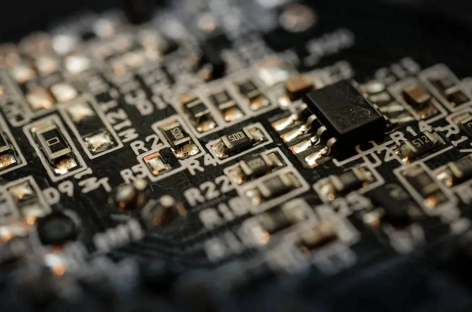
Standard PCB Design Workflow for Engineers
Standardized PCB design workflow detailing preparation, netlist/mechanical import, placement, stackup, routing, DRC and Gerber verification for manufacturable PCB designs.
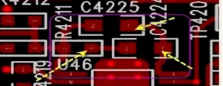
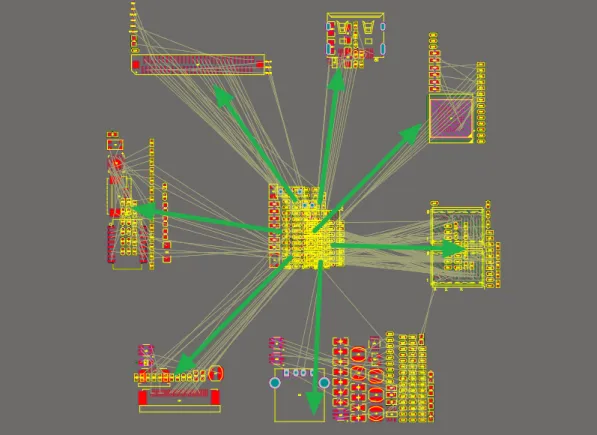
Power Module PCB Design: From Theory to Practice
Guide to PCB design for switching regulator and LDO power modules: layout, grounding, thermal and EMI mitigation, component placement and copper pour practices.
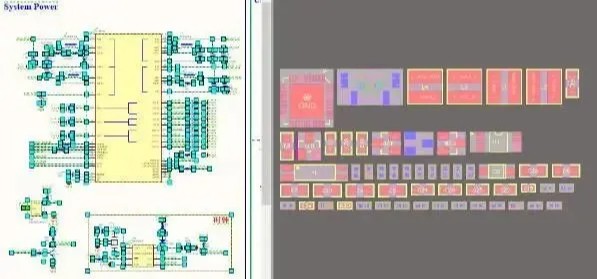
Interactive and Modular PCB Layouts to Double Design Efficiency
Practical guide to interactive layout and modular layout in PCB design: use Cross Select Mode and Arrange Components Inside Area to speed component placement.
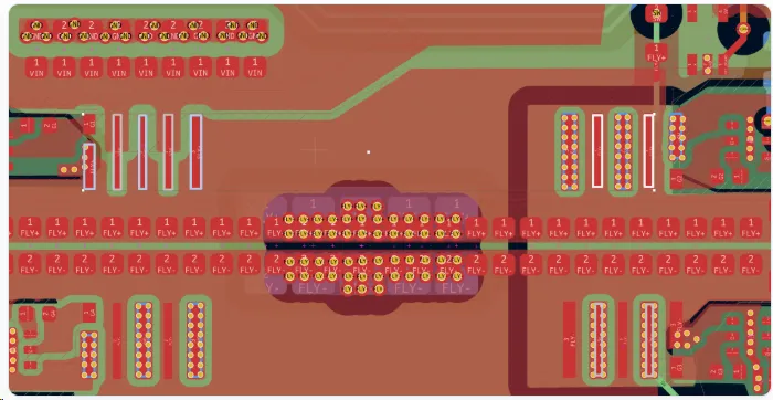
Fill Resistance Plugin: Measured Copper Pour Resistance and PDN Voltage Drop
Fill Resistance is a KiCad plugin that computes DC copper resistance, current density, per-via currents and power loss for copper pours, with a PDN mode for multi-source analysis.
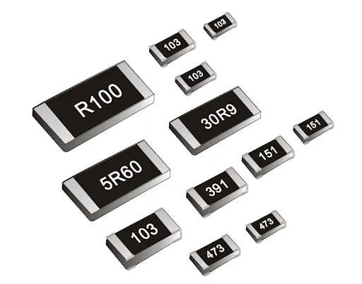
SMD Resistor Codes and Resistance Value Calculations
Technical guide to SMD resistor codes: three- and four-digit formats, 'R' decimal notation, EIA-96 high-precision scheme, plus lookup tables and practical examples.
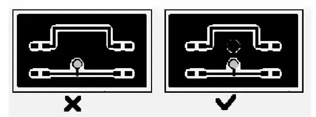
Core Principles of PCB Design
PCB routing guidelines for engineers: routing priority, impedance control and termination, and signal integrity practices to minimize crosstalk and EMC issues.
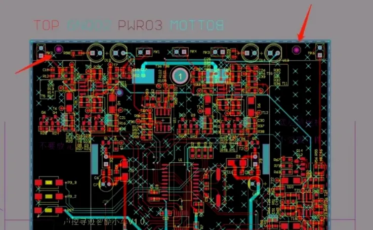
PCB Fiducials: Small Marks That Impact Production
Technical guide to fiducials in PCB design: their five manufacturing roles and practical 1-2-3 sizing and placement rules, including three marks per component side.
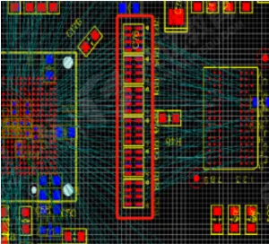
How a Series Resistor on a PCB Improves Signal Integrity
Explains why a series resistor is used on PCB signal lines, how it damps reflections and aids impedance matching, plus practical guidelines for selecting values.


