


PCB Design
Printed Circuit Board (PCB) design forms the backbone of modern electronics, enabling the creation of compact, efficient, and reliable devices that power everything from smartphones to industrial machinery. In this category, readers gain access to a comprehensive collection of resources dedicated to mastering PCB design principles and techniques. Whether you are a seasoned engineer refining complex layouts or a newcomer learning the fundamentals, these articles provide the knowledge needed to tackle real-world challenges in electronics development. The scope of PCB design covered here extends from initial schematic capture to final board fabrication and testing. Articles delve into essential topics such as layer stacking, signal integrity, thermal management, and component placement strategies. Guides and tutorials offer step-by-step instructions for using popular software tools like Altium Designer and KiCad, while insights explore emerging trends like flexible PCBs and high-speed designs. Best practices emphasize error reduction, cost optimization, and compliance with industry standards, ensuring designs are not only functional but also manufacturable at scale. Real-world applications highlight the category's practical value, demonstrating how effective PCB design contributes to innovations in automotive systems, medical equipment, renewable energy solutions, and consumer gadgets. By addressing common pitfalls and sharing expert tips, these pieces equip professionals to enhance product performance and reliability. Readers benefit from building a deeper understanding through interconnected articles that cover foundational concepts alongside advanced methodologies, fostering continuous improvement in electronics projects. For those involved in prototyping or production, the technical relevance of this content lies in its focus on efficiency and innovation. Detailed discussions on impedance control, EMI shielding, and design for manufacturability prepare you to meet the demands of today's fast-paced tech landscape. Engaging with multiple articles in this category allows for a progressive learning path, where foundational knowledge supports exploration of specialized topics, ultimately leading to more robust and innovative PCB designs.
Featured Blog
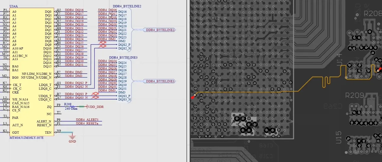
PCB Design Review for Beginners: A Step by Step Guide
Learn how to perform a PCB design review with a practical checklist covering schematics, layout, DRC, manufacturability, and pre-production checks.
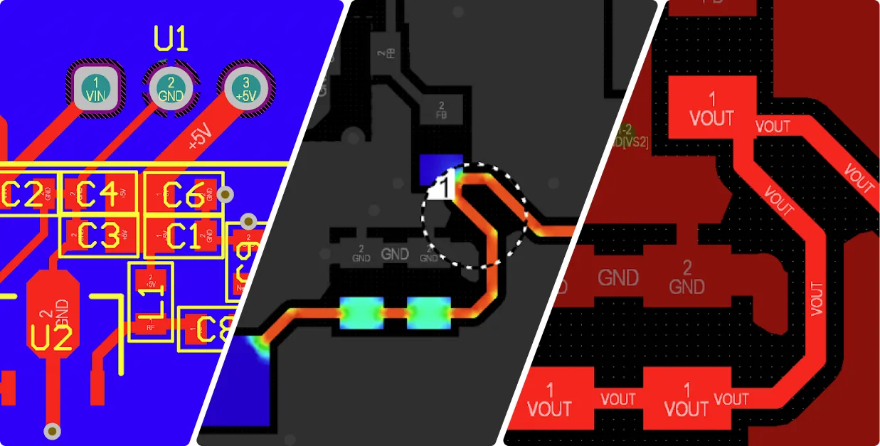
Latest Blogs
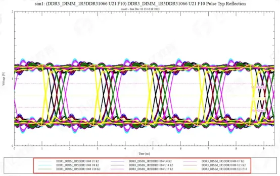
DDR Signal Integrity: Effects of Termination Resistors
DDR3 fly-by analysis: SigXplorer eye-diagram comparison shows far-end termination resistor preserves signal integrity by damping reflections and widening timing margin.
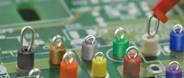
5 Practical ESD Design Tips
Practical ESD protection guide for engineers: grounding strategies, suppressors, shielding, PCB layout best practices and targeted components to reduce ESD failures.
Testing SW Signals in DC-DC Converters
Practical methods to verify SW signal integrity in DC-DC converters: oscilloscope observation, spectrum and load-response analysis, TDR and crosstalk testing for reliability.
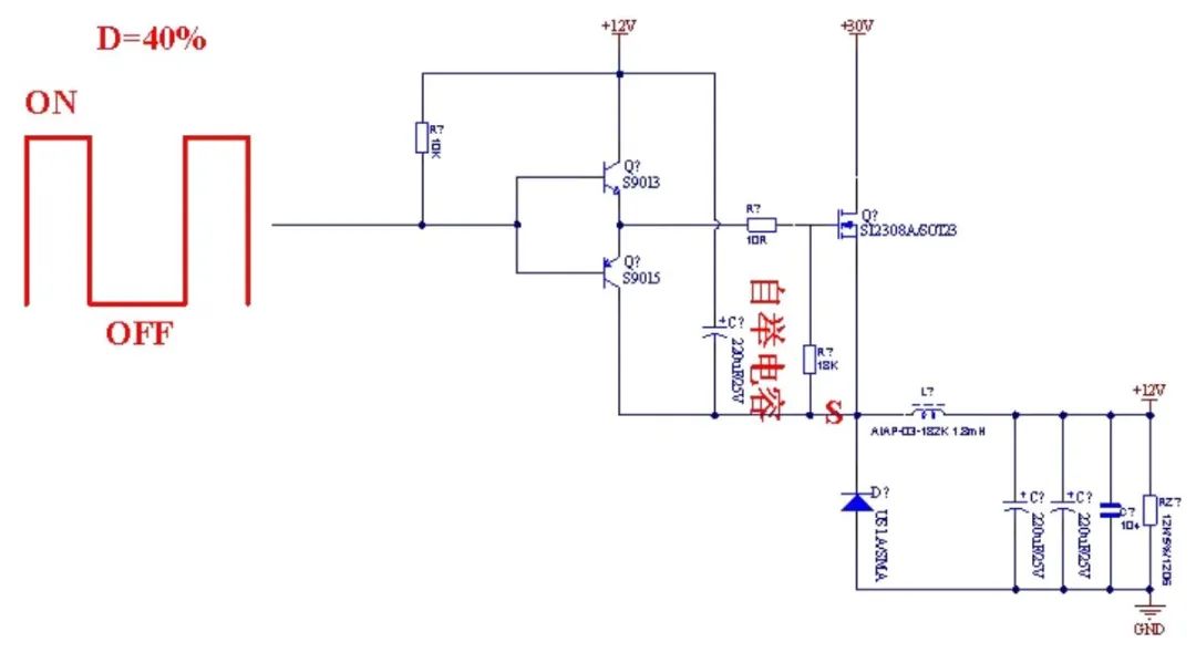
BUCK Converter Hysteretic Circuit: From Principle to Parameter Calculation
Design a BUCK hysteretic comparator with a 12 V push-pull MOSFET drive, 4 V/8 V thresholds, LM393DT, resistor divider values, and a 1 nF timing capacitor at 20 kHz.
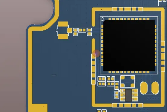
A PCB Shield Can Is Not Just a Metal Lid
A shield can is an EMI isolation volume, not a lid. Plan clips, ground, and access for power, core, and wireless modules before EMI testing forces a late change.
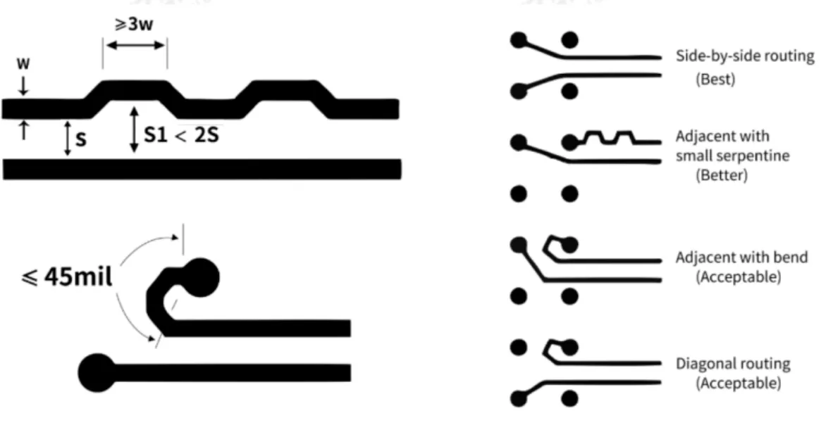
PCB Layout and Routing Requirements for a DP 1.4 Interface
DP 1.4 PCB rules: BGA ground vias, fence gap ≥ 4W, 6 mil intra-pair match, ≥ 8 Gbps connector practice, and ground-plane voids under pads with two GND vias each.
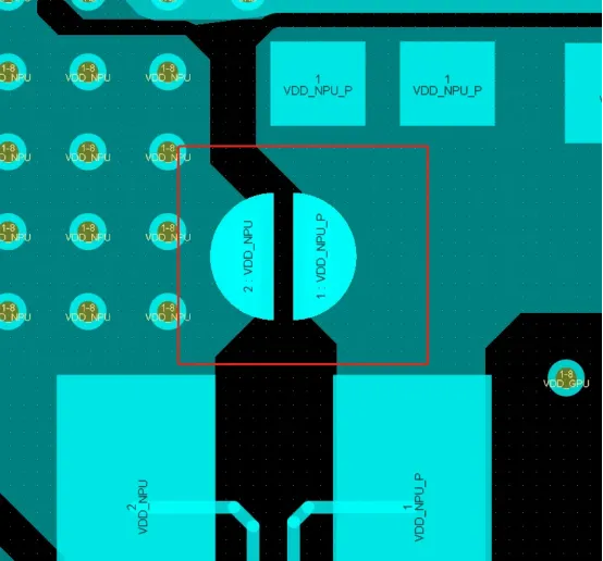
PCB Jumpers: Types, Functions, and Correct Use
PCB jumpers include wire, resistor, solder-blob, and hole styles. Keep them short, off sensitive nets, well soldered, and continuity-tested to avoid noise and opens.
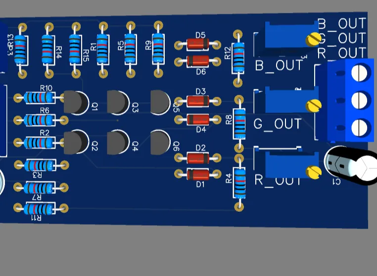
VGA OUT PCB Design: Key Layout and Routing Rules
VGA OUT layout rules: short analog runs, 75 Ω 1% pulldowns, 12 mil RGB with 200 mil match, ground fencing, ground reference, and connector-side TVS with no stubs.
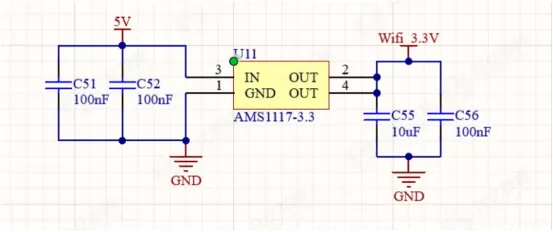
LDO Power PCB Design: From the Regulator Circuit to Placement and Routing
LDO PCB layout for AMS1117-3.3: in-line or L placement, large-then-small caps, current-sized traces, vias around the filters, and a shared input-output ground.
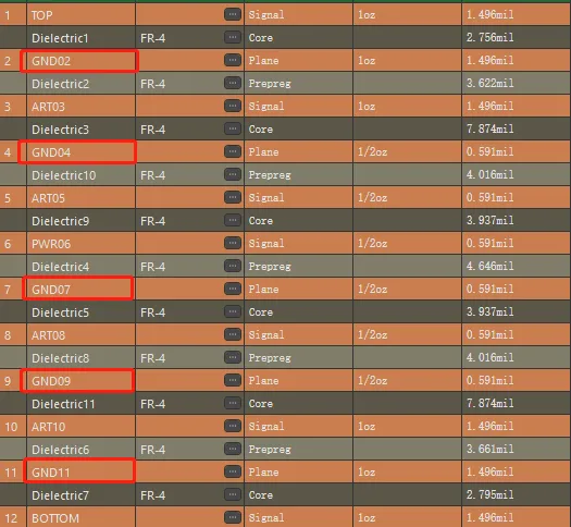
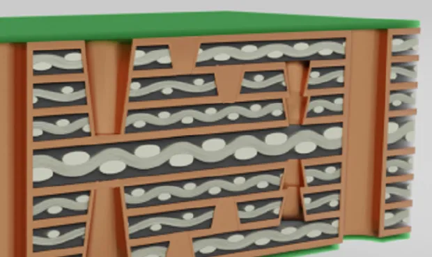
Stack-up Principles for Multilayer PCB Design
Multilayer PCB stack-up rules: pair signals with ground, keep the stack symmetric, put ground under parts, place power next to ground, and avoid parallel adjacent routing layers.

Five ESD Design Practices That Reduce Discharge Damage
Five ESD practices: common grounding, TVS and MOV suppressors, shielding materials, PCB layout that avoids high-impedance paths, and diodes at I/O and antenna ports.
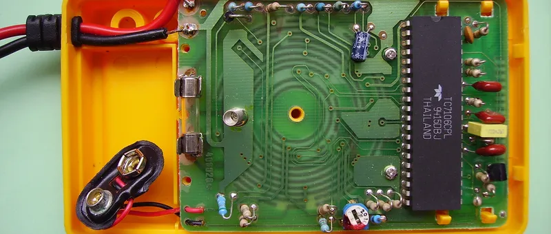
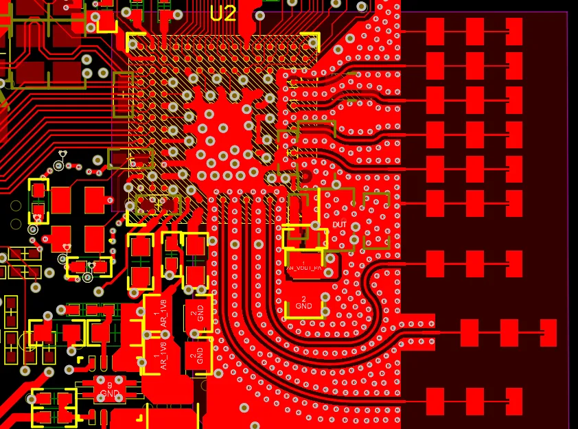
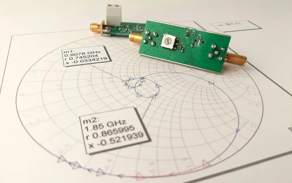
Why a Bare-Board 50 Ω Trace Reads Lower After Solder Mask
Why a bare-board 50 Ω microstrip reads lower after solder mask: higher effective Dk, no single ohm offset, coupon vs finished state, and one-variable TDR debug.


