 00:51
00:51
Via Plugging
Via plugging is a critical process in printed circuit board (PCB) manufacturing that involves filling or capping the vias—small holes that connect different layers of a PCB—to enhance performance, reliability, and manufacturability. For engineers, designers, and hobbyists searching for information on via plugging, this tag serves as a comprehensive resource, covering everything from basic techniques to advanced applications in high-density interconnect (HDI) boards and multilayer designs. One of the primary reasons to implement via plugging is to prevent issues like solder wicking, where molten solder flows into unfilled vias during assembly, potentially causing shorts or voids. By plugging vias with materials such as epoxy resin or conductive inks, you can improve thermal management, reduce signal interference, and ensure better structural integrity, especially in environments exposed to moisture, dust, or mechanical stress. This technique is particularly valuable in industries like aerospace, automotive, and consumer electronics, where compact, reliable PCBs are essential. For instance, in high-frequency applications, plugged vias minimize electromagnetic interference and support finer pitch components, leading to more efficient designs. When considering via plugging in your projects, focus on best practices such as selecting the appropriate plugging method—whether tenting, filling, or capping—based on board thickness, via size, and end-use requirements. It's also important to adhere to standards like IPC-4761, which outline guidelines for via protection to avoid common pitfalls like incomplete filling or material shrinkage. Proper implementation can significantly extend the lifespan of your PCBs and reduce failure rates during production and operation. The articles under this Via Plugging tag delve into these topics with practical examples, step-by-step tutorials, and case studies, helping you apply these concepts effectively in your own work. Whether you're troubleshooting a design flaw or optimizing a new prototype, the insights here can guide your decisions and improve outcomes.
Video Guide
-
00:51
Technical Articles

6-Layer FR-4 PCB Engineering Case Study: Solder Mask Bridge and Via Plugging Conflicts in CAM Review
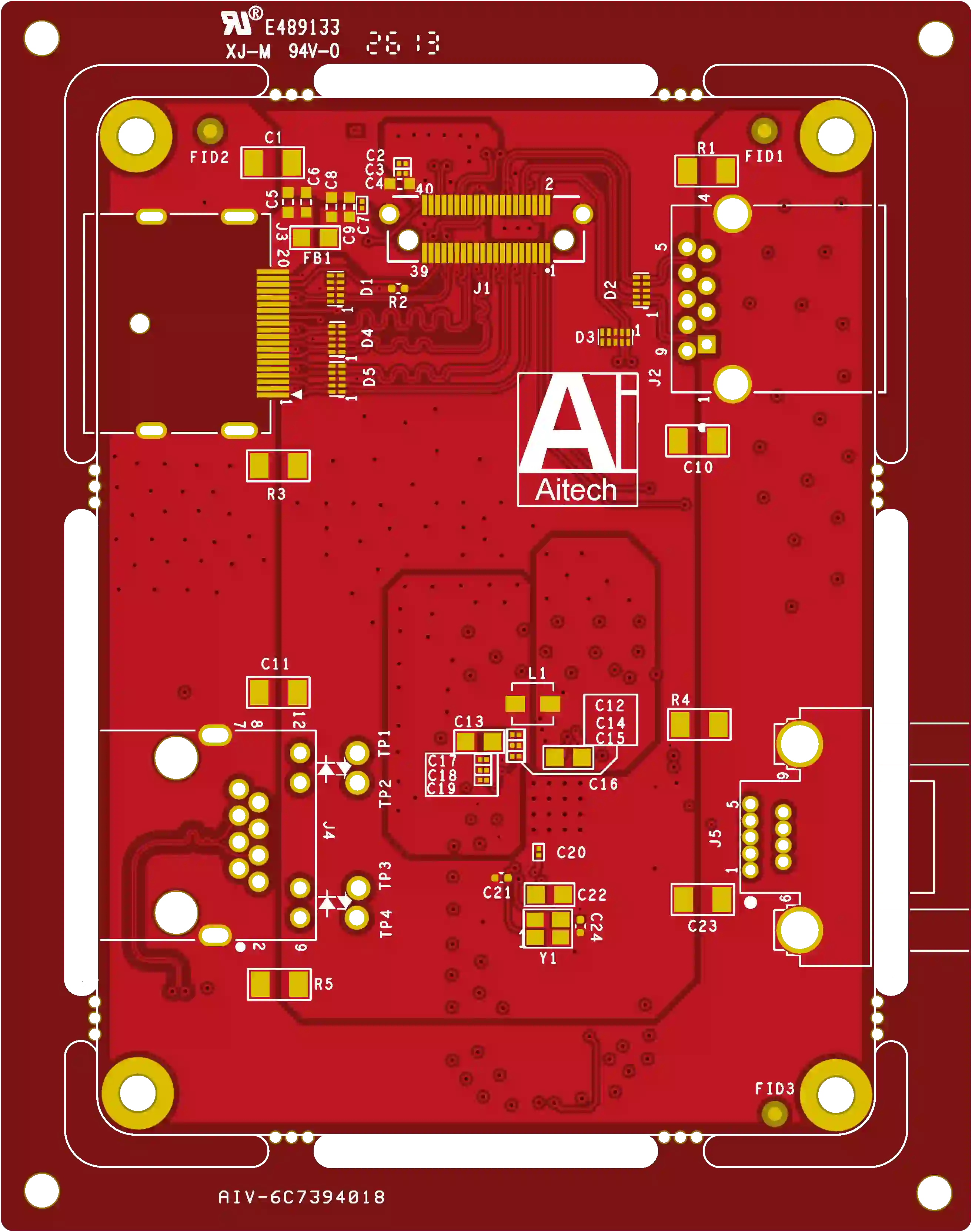
How to Fix Solder Mask Bridge and Via Issues in 6-Layer PCBs
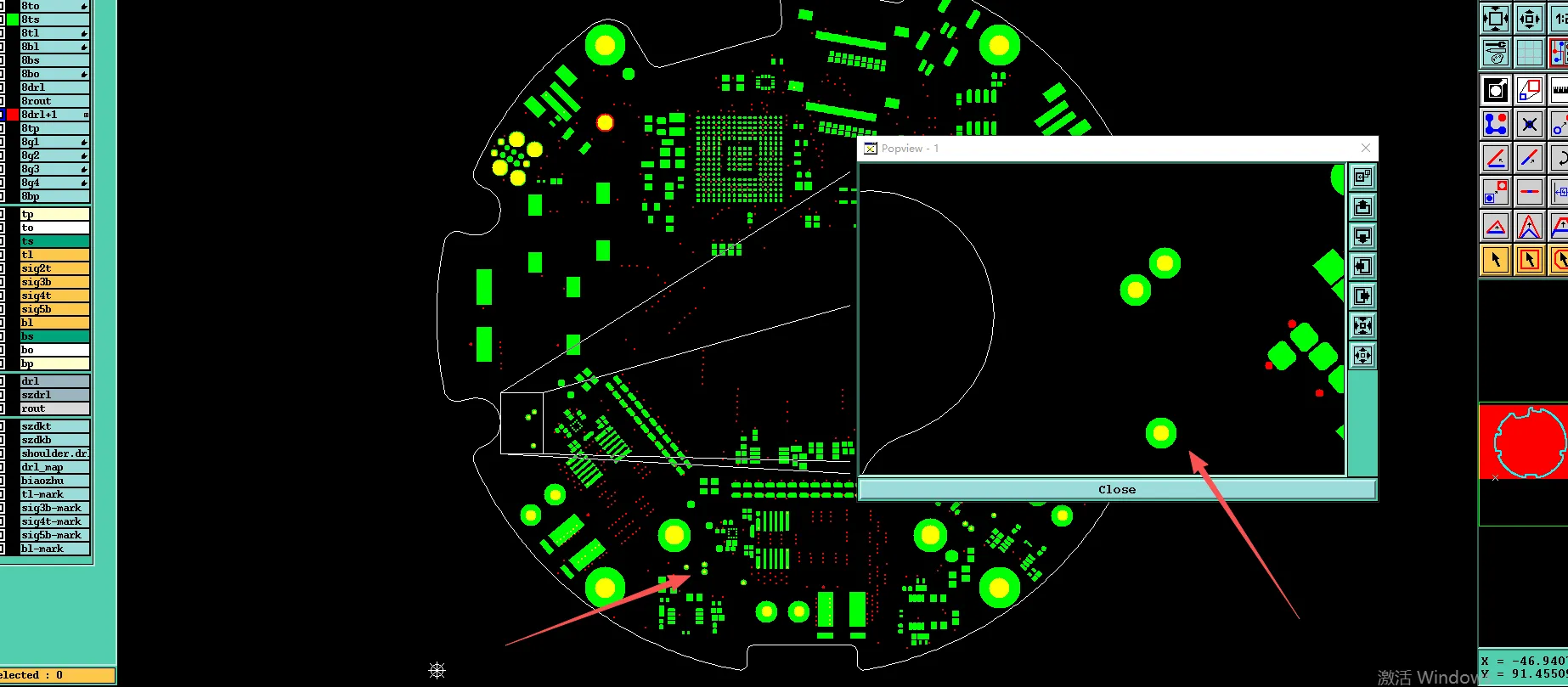
Avoiding DFM Delays: A Guide to PCB Resin Filled Via Design
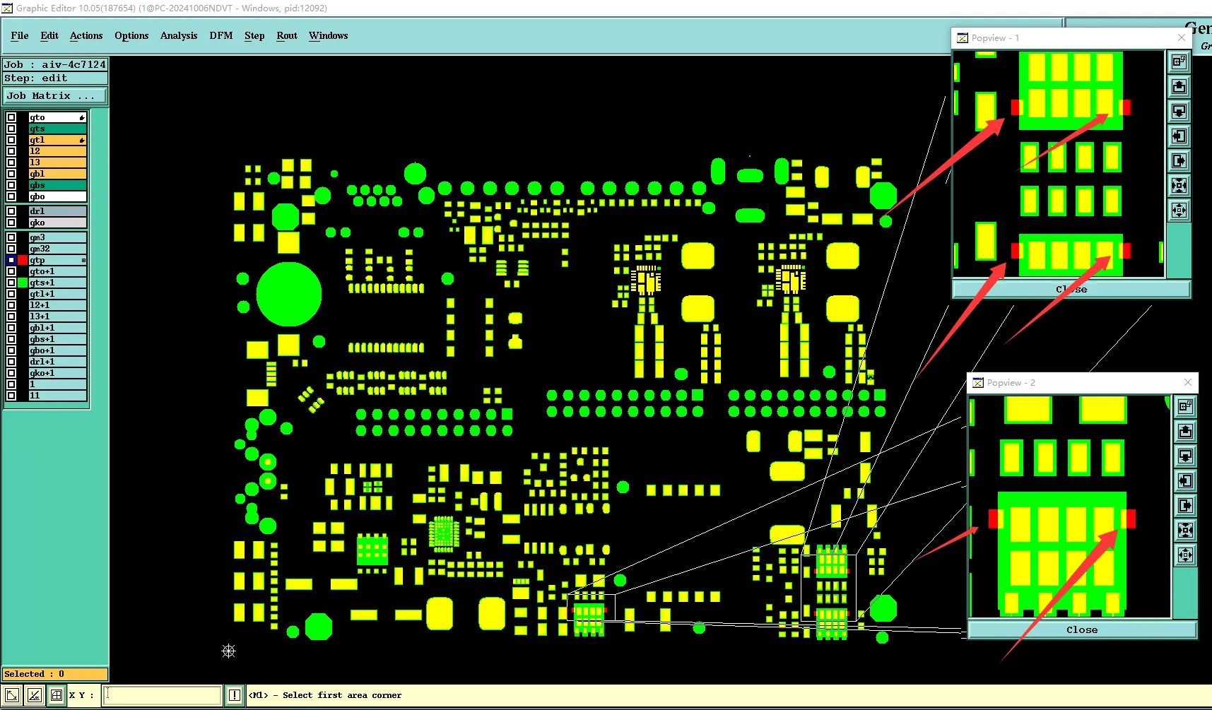
Solder Mask vs. Paste Mask: Perfecting Your Opening Design
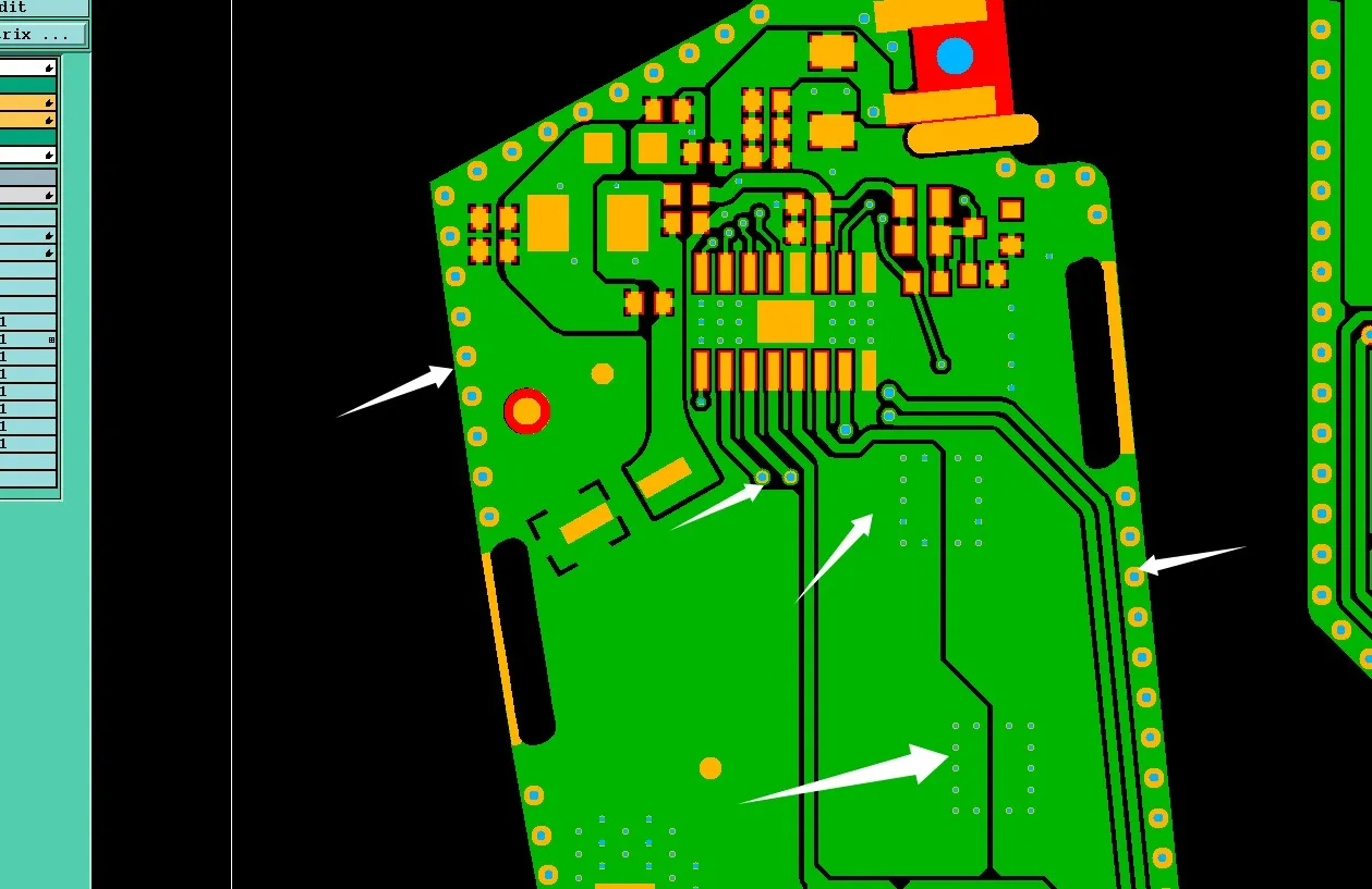
How We Resolved PCB Solder Mask Opening Design Conflicts in a 2-Layer FR4 PCB
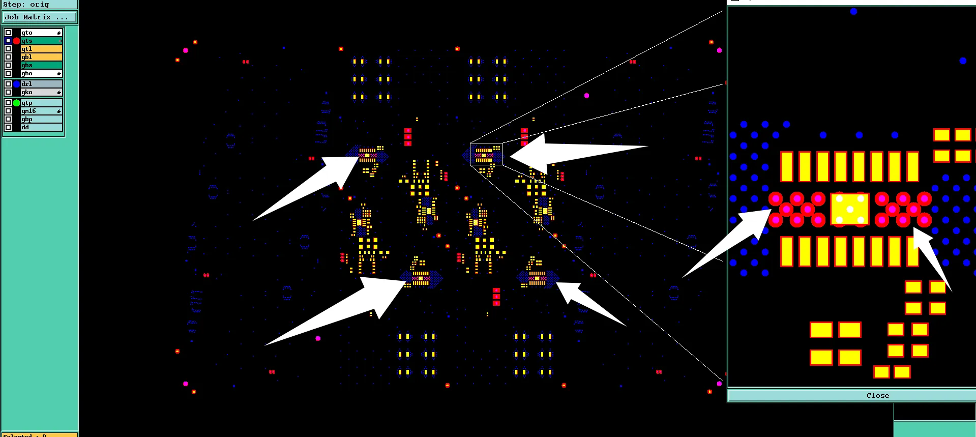
Resolving Tented Via vs Open Via Mismatches in PCB Manufacturing
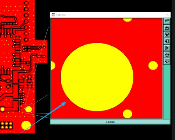
Preventing Exposed Copper and Via Plugging Risks in a Compact 4-Layer FR4 PCB
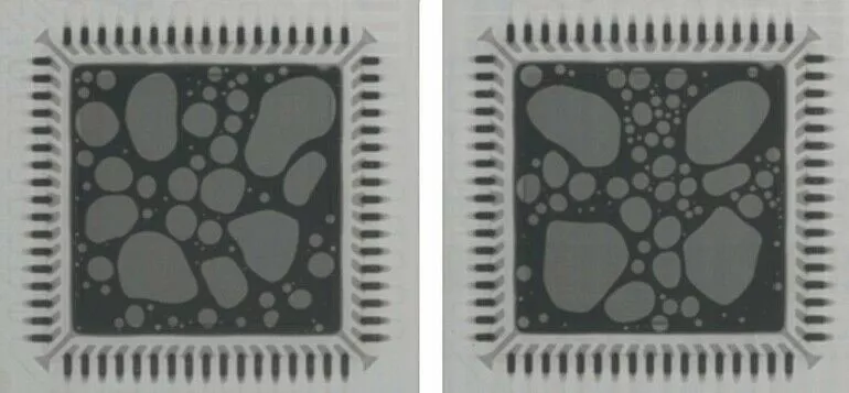
Thermal Pad Design for QFN Packages: Best Practices for Void Reduction
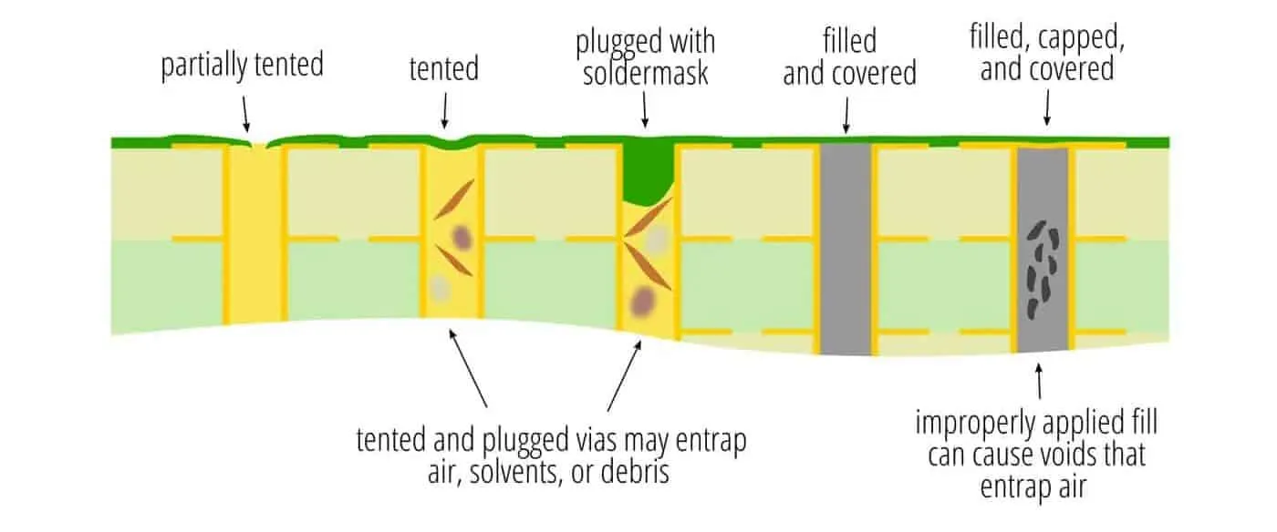
Overcoming Solder Wicking in Via in Pad: Techniques and Solutions
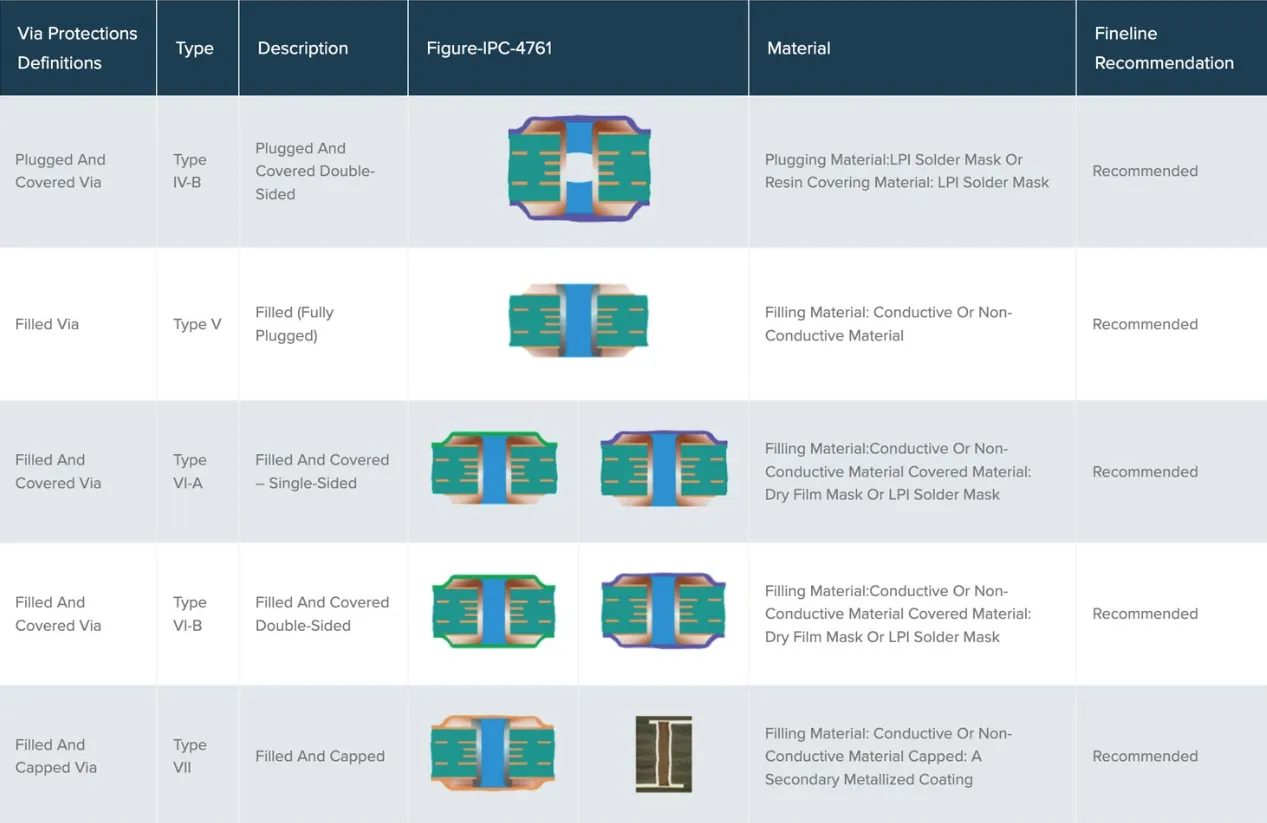
A Beginner's Guide to PCB Via Filling: Understanding the Basics
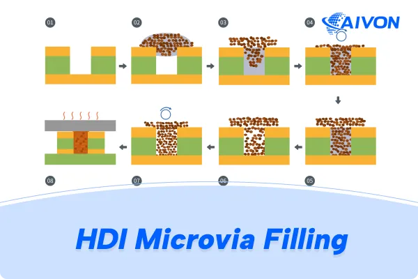
The Ultimate Guide to PCB Microvia Filling: Materials, Methods, and Reliability Considerations
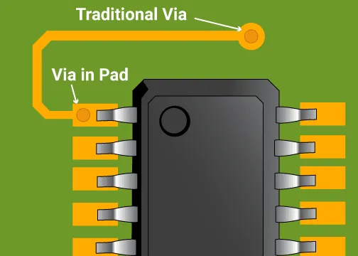
Troubleshooting Common Via-in-Pad Issues in PCB Design
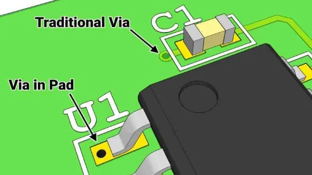
FR4 PCB Via-in-Pad: Benefits, Risks, and Design Considerations
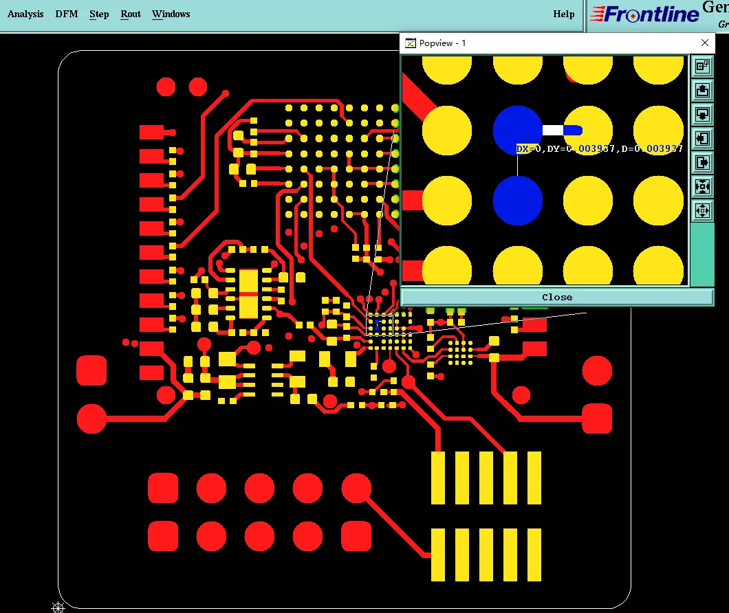
PCB Solder Mask and Via Design Issues: What CAM Review Commonly Finds
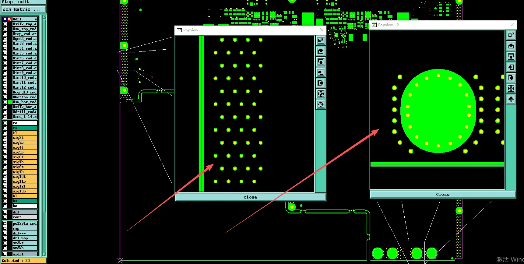
How We Resolved Resin Plug Tenting Conflict on 14-Layer PCB
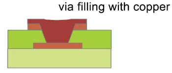
Copper-Filled vs Resin-Filled Vias in HDI PCB: Which Should You Use?
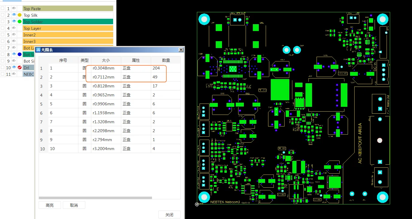
How DFM Prevented Via Tenting Issues in 4-Layer FR4 PCB
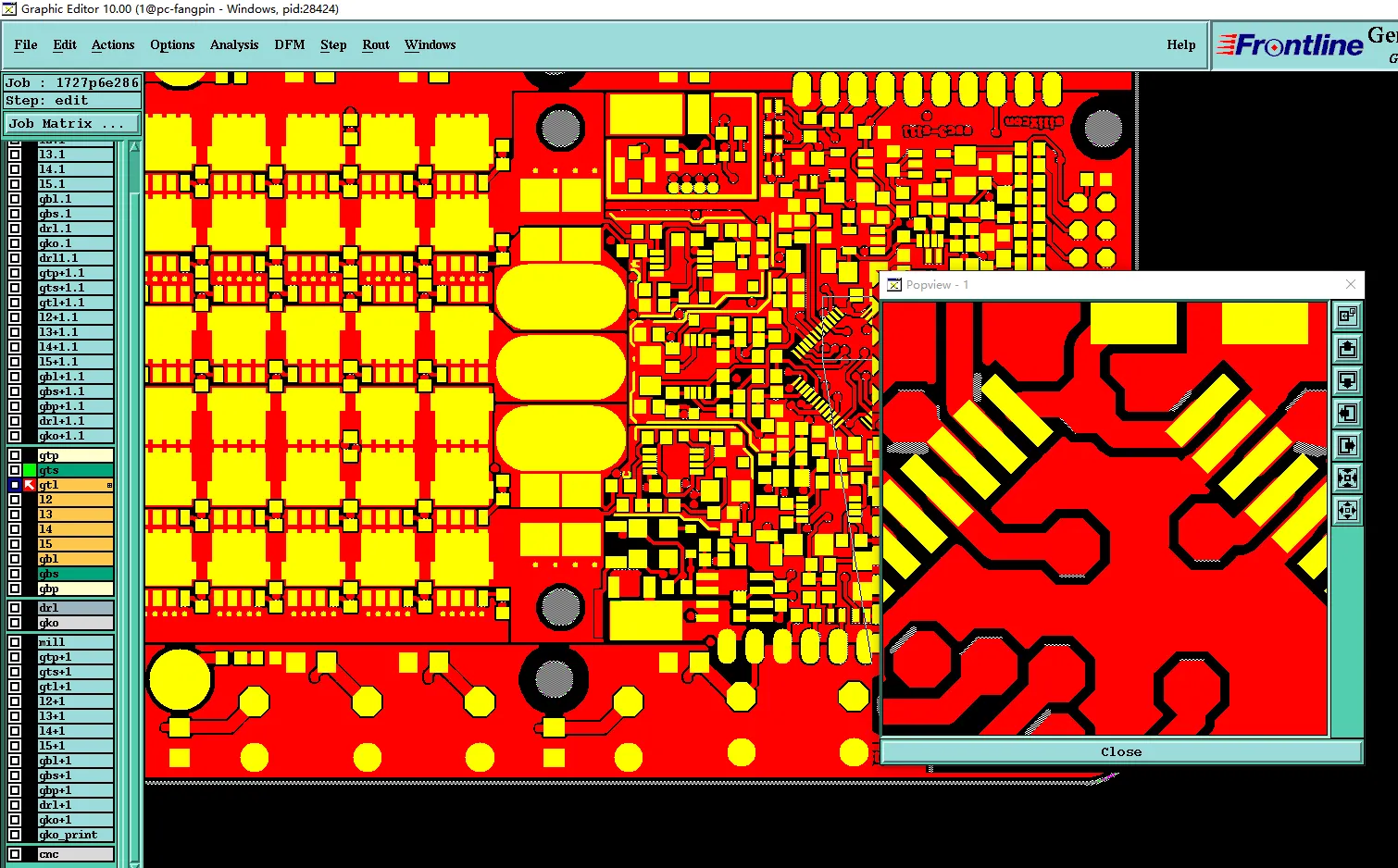
How DFM Prevented Heavy Copper Etch Failures in Multilayer PCB

How to Avoid Common Engineering Queries in Multilayer FR4 PCB Design