 00:45
00:45
HDI Design
High Density Interconnect (HDI) design represents a critical advancement in printed circuit board (PCB) technology, enabling the creation of compact, high-performance electronics with intricate layering and fine-pitch components. This tag focuses on the principles, techniques, and innovations in HDI design, which are essential for engineers and designers tackling modern challenges in miniaturization and signal integrity. By incorporating microvias, buried vias, and sequential lamination, HDI boards support higher component density and improved electrical performance, making them ideal for applications in smartphones, medical devices, automotive systems, and aerospace equipment. For professionals searching for HDI design guidance, this collection offers practical insights into optimizing layer stacks, selecting appropriate materials, and implementing via-in-pad structures to reduce signal loss and enhance reliability. Key best practices include careful consideration of thermal management to prevent overheating in dense configurations, as well as adherence to manufacturing tolerances to ensure yield rates remain high. Understanding these elements can help mitigate common pitfalls, such as crosstalk or impedance mismatches, leading to more efficient prototyping and production cycles. Whether you are refining an existing design or starting a new project, the articles under this HDI design tag provide detailed case studies and step-by-step methodologies drawn from industry expertise. Delving into these resources can equip you with the knowledge to achieve superior functionality in space-constrained environments, ultimately driving innovation in your electronic products.
Video Guide


Technical Articles
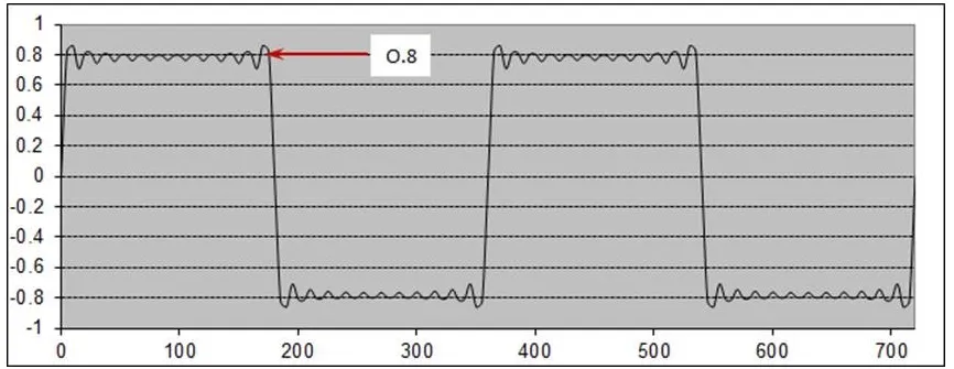
Why HDI PCB Trace Width Changes During Routing Can Cause Problems
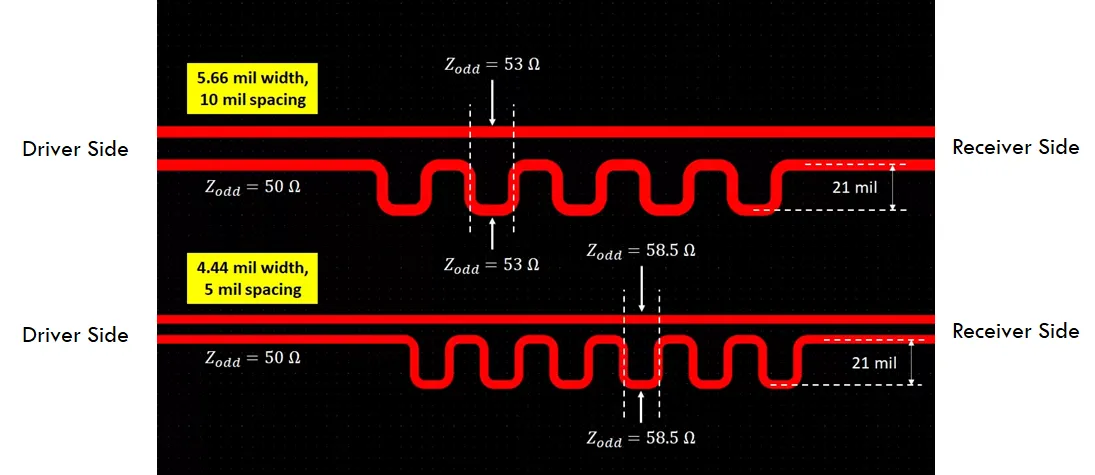
HDI Differential Pair Spacing: Common Layout Mistakes to Avoid
HDI PCB Copper Balance: Why Uneven Copper Distribution Matters
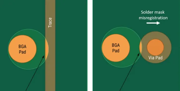
HDI BGA Pad Clearance Problems That Can Delay Production
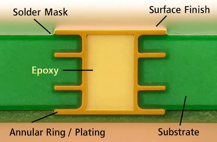
How to Avoid Solder Mask Issues Around HDI Microvias
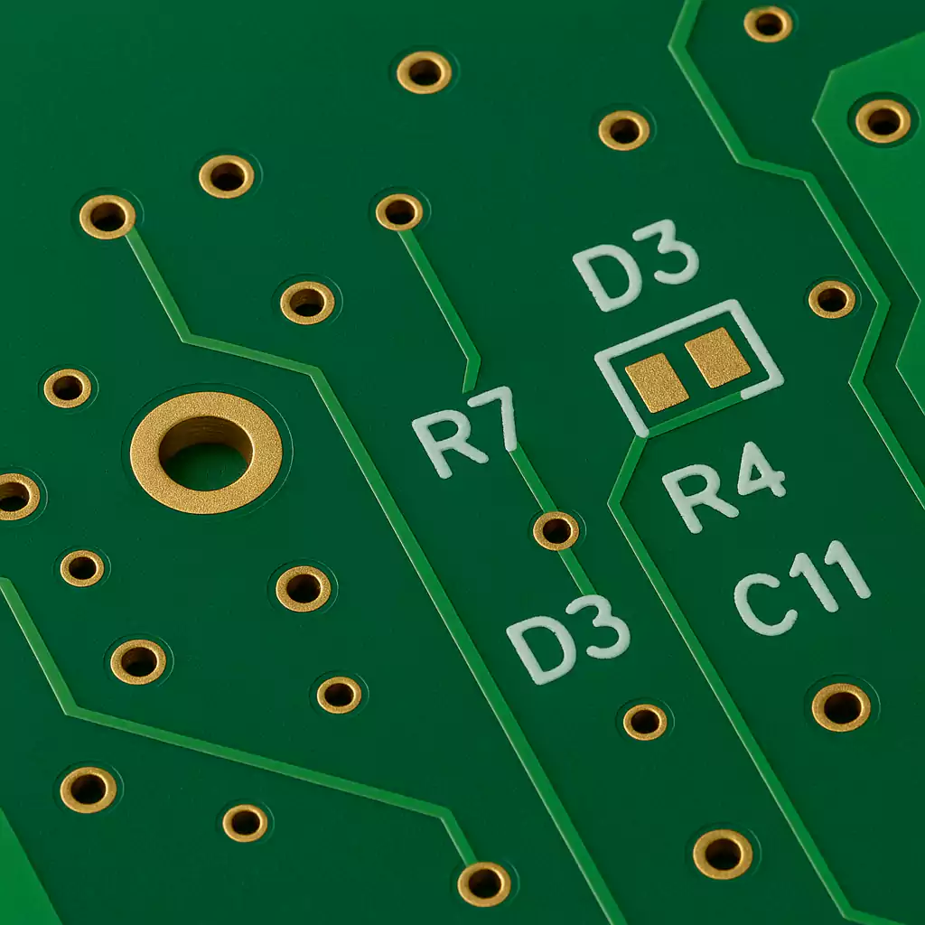
HDI Solder Mask Expansion: Common CAM Review Problems
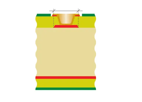
Why Microvia Landing Pads Fail During HDI Manufacturing
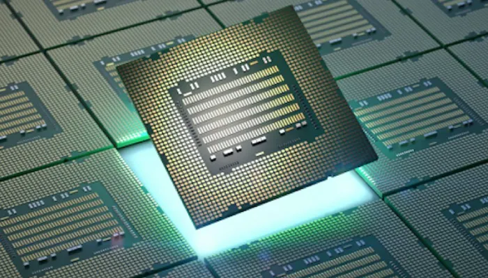
HDI PCB Applications: Powering Miniaturization, Performance, and Reliability Across Industries

The Significance of Via Placement in BGA Fanout Designs
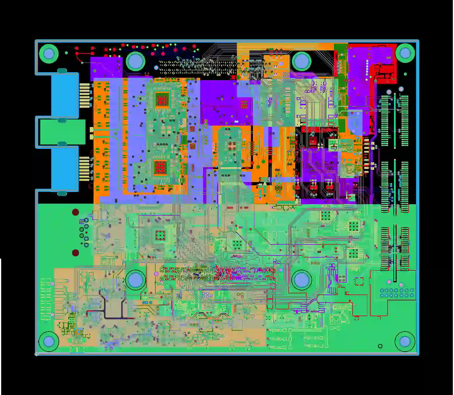
Common PCB CAM Review Engineering Queries in Multilayer HDI PCB Design
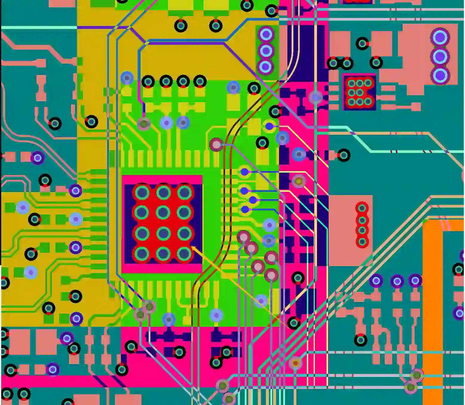
Common Engineering Issues in HDI PCB Manufacturing with Different Surface Finishes

Compact VR: Miniaturization Techniques for Headset PCBs
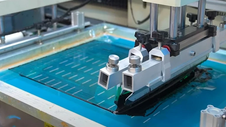
Silk Screen Color and High-Density PCBs: Optimizing for Clarity

Miniaturization Matters: Designing Compact Avionics System PCBs for Weight Reduction